

Inter‐Layer Diffusion of Excitations in 2D Perovskites Revealed by Photoluminescence Reabsorption
Advanced Functional Materials Wiley (2025) 2421817
Abstract:
2D lead halide perovskites (2DPs) offer chemical compatibility with 3D perovskites and enhanced stability, which are attractive for applications in photovoltaic and light‐emitting devices. However, such lowered structural dimensionality causes increased excitonic effects and highly anisotropic charge‐carrier transport. Determining the diffusivity of excitations, in particular for out‐of‐plane or inter‐layer transport, is therefore crucial, yet challenging to achieve. Here, an effective method is demonstrated for monitoring inter‐layer diffusion of photoexcitations in (PEA)2PbI4 thin films by tracking time‐dependent changes in photoluminescence spectra induced by photon reabsorption effects. Selective photoexcitation from either substrate‐ or air‐side of the films reveals differences in diffusion dynamics encountered through the film profile. Time‐dependent diffusion coefficients are extracted from spectral dynamics through a 1D diffusion model coupled with an interference correction for refractive index variations arising from the strong excitonic resonance of 2DPs. Such analysis, together with structural probes, shows that minute misalignment of 2DPs planes occurs at distances far from the substrate, where efficient in‐plane transport consequently overshadows the less efficient out‐of‐plane transport in the direction perpendicular to the substrate. Through detailed analysis, a low out‐of‐plane excitation diffusion coefficient of (0.26 ± 0.03) ×10−4 cm2 s−1 is determined, consistent with a diffusion anisotropy of ≈4 orders of magnitude.Unlocking photoanode performance through a roadmap for electrophoretic deposition of carbon nitride/tungsten oxide heterojunction thin films
Materials Advances Royal Society of Chemistry 6:12 (2025) 4106-4114
Abstract:
The formation of high-quality semiconductor thin films is a significant challenge that requires precise control over various factors, including film thickness, uniformity, crystallinity, and strong adhesion to the underlying substrate. These parameters are particularly critical in photoelectrode fabrication, where the thin film must efficiently interact with incident light to maximise absorption and facilitate effective photogenerated charge separation and transport to improve the overall photoelectrochemical performance. In this work, we systematically investigate the formation of graphitic carbon nitride/tungsten oxide (g-C3N4/WO3) hybrid material thin film using electrophoretic deposition (EPD). Transmission electron microscopy reveals direct contact between g-C3N4 and WO3, while X-ray photoelectron spectroscopy indicates electron transfer from g-C3N4 to WO3, confirming the formation of an effective n–n-heterojunction at the interface. We identified four key EPD coating parameters that affect the thin film quality and photoanode performance, including substrate pretreatment, suspension solvent, deposition voltage and time, and post-annealing. Notably, the dispersion of g-C3N4/WO3 heterojunction particles in acetone, in the presence of iodine, results in an excellent film compared to those prepared in water and isopropanol. The most important parameter is the thickness of the film, which must be optimal for light absorption and charge separation: if the film is too thin, it absorbs insufficient light; conversely, if it's too thick, the photogenerated charge carriers recombine before reaching the electrode or electrolyte. By exploring a range of conditions, we determined the optimal substrate surface chemistry and identified acetone as the best solvent with a suspension concentration of 3 mg mL−1. The ideal deposition parameters were a voltage of 60 V for 10 seconds, and post-annealing at 300 °C for 2 hours in air. These optimised conditions allowed us to maximise the functional characteristics of the resulting photoanode, achieving a photocurrent density of 0.2 mA cm−2 at 1.23 V vs. RHE, which outperformed other carbon nitride-based materialsResonance-Amplified Terahertz Near-Field Spectroscopy of a Single Nanowire
Nano Letters American Chemical Society 24:49 (2024) 15716-15723
Abstract:
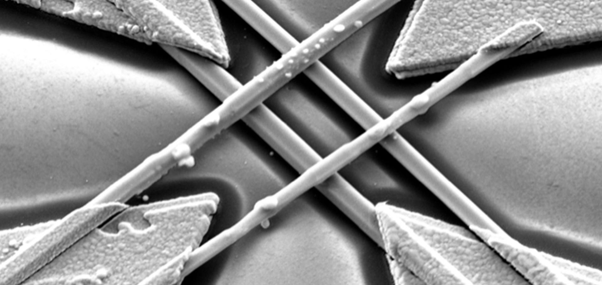
Nanoscale material systems are central to next-generation optoelectronic and quantum technologies, yet their development remains hindered by limited characterization tools, particularly at terahertz (THz) frequencies. Far-field THz spectroscopy techniques lack the sensitivity for investigating individual nanoscale systems, whereas in near-field THz nanoscopy, surface states, disorder, and sample-tip interactions often mask the response of the entire nanoscale system. Here, we present a THz resonance-amplified near-field spectroscopy technique that can detect subtle conductivity changes in isolated nanoscale systemssuch as a single InAs nanowireunder ultrafast photoexcitation. By exploiting the spatial localization and resonant field enhancement in the gap of a bowtie antenna, our approach enables precise measurements of the nanostructures through shifts in the antenna resonant frequency, offering a direct means of extracting the system response, and unlocking investigations of ultrafast charge-carrier dynamics in isolated nanoscale and microscale systems.A thorough experimental assessment of THz-TDS plasma diagnostic techniques for nuclear fusion applications
Review of Scientific Instruments AIP Publishing 95:10 (2024) 103519
Alumina nanoparticles enable optimal spray-coated perovskite thin film growth on self-assembled monolayers for efficient and reproducible photovoltaics
Journal of Materials Chemistry C Royal Society of Chemistry (RSC) 12:34 (2024) 13332-13342