

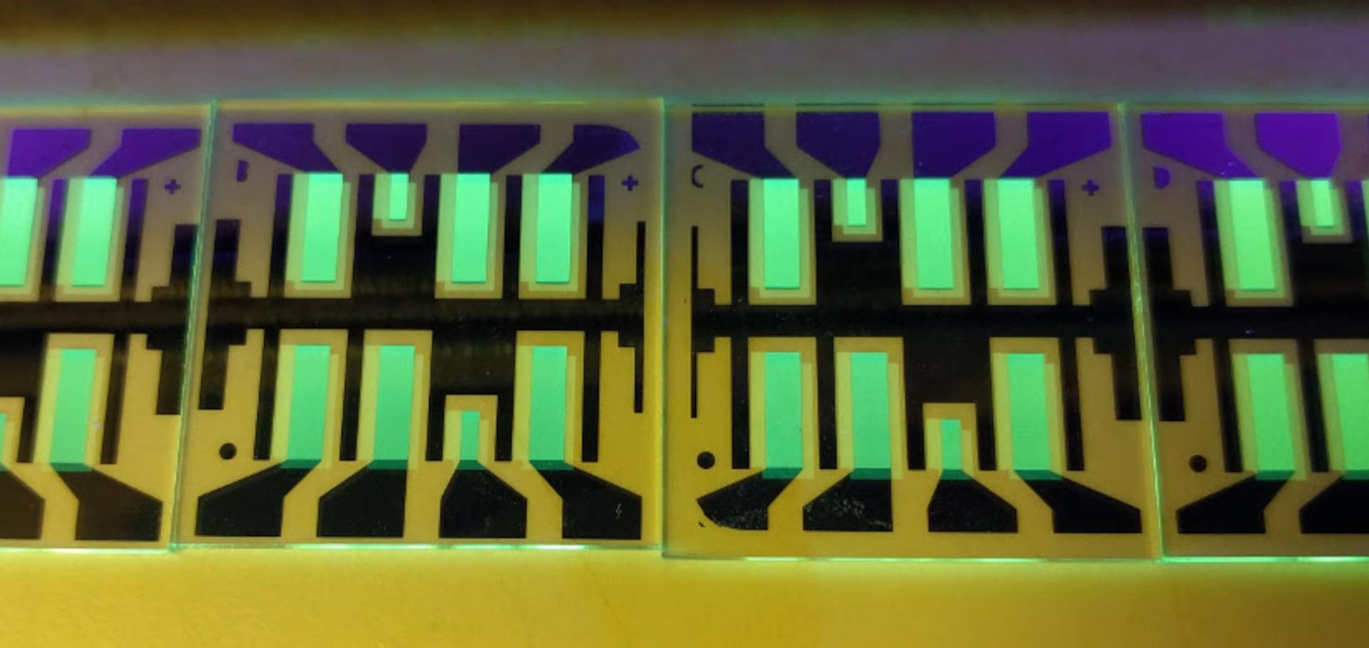

Ultrafast Charge Dynamics in Dilute-Donor versus Highly Intermixed TAPC:C60 Organic Solar Cell Blends.
The journal of physical chemistry letters (2020)
Abstract:
Elucidating the interplay between film morphology, photophysics, and device performance of bulk heterojunction (BHJ) organic photovoltaics remains challenging. Here, we use the well-defined morphology of vapor-deposited di-[4-(N,N-di-p-tolyl-amino)-phenyl]cyclohexane (TAPC):C60 blends to address charge generation and recombination by transient ultrafast spectroscopy. We gain relevant new insights to the functioning of dilute-donor (5% TAPC) fullerene-based BHJs compared to molecularly intermixed systems (50% TAPC). First, we show that intermolecular charge transfer (CT) excitons in the C60 clusters of dilute BHJs rapidly localize to Frenkel excitons prior to dissociating at the donor:acceptor interface. Thus, both Frenkel and CT excitons generate photocurrent over the entire fullerene absorption range. Second, we selectively monitor interfacial and bulk C60 clusters via their electro-absorption, demonstrating an energetic gradient that assists free charge generation. Third, we identify a fast (< 1 ns) recombination channel, whereby free electrons recombine with trapped holes on isolated TAPC molecules. This can harm the performance of dilute solar cells, unless the electrons are rapidly extracted in efficient devices.In Situ Observations of the Growth Mode of Vacuum-Deposited alpha-Sexithiophene
JOURNAL OF PHYSICAL CHEMISTRY C 124:22 (2020) 11863-11869
Abstract:
© 2020 American Chemical Society. The real-time morphological evolution of vacuum-deposited α-sexithiophene (α-6T) on a weakly interacting (glass) substrate at ambient temperature is reported. In situ grazing-incidence small-angle X-ray scattering (GISAXS) enabled the observation of nanoscale aggregates, while in situ grazing-incidence wide-angle scattering (GIWAXS) allowed the study of the molecular-scale morphology. The in situ GISAXS measurements revealed that the α-6T growth proceeds via a Stranski-Krastanov mode, whereby 2-4 complete monolayers are deposited, followed by subsequent layers formed via island growth. In situ GIWAXS also showed the evolution of the polymorph composition during the thin-film growth. Initially, the disordered β-phase and the low-temperature (LT)-phase are deposited in nearly equal proportion until a thickness of 8 nm, whereby the LT-phase begins to dominate until a final α-6T thickness of 50 nm where the scattering intensity of the LT-phase is more than double that of the β-phase. The change in the polymorph composition coincided with an increase in the LT-phase d-spacing, indicating a lattice strain relief as the thin film moves from surface to bulk-mediated growth. The GISAXS findings were confirmed through direct imaging using ex situ atomic force microscopy (AFM) at various thicknesses, revealing the existence of both initial the initial and intermediate monolayers and final island morphologies. The findings reveal the real-time morphological evolution of α-6T across both the molecular scale and the nanoscale and highlight the role of strain in polymorph growth. Due to the importance of the thin-film microstructure in device performance, it is expected that these results will aid in the development of structure-property relationships necessary to realize the full potential of organic electronics.Efficiency enhancement of small molecule organic solar cells using hexapropyltruxene as an interface layer
JOURNAL OF MATERIALS CHEMISTRY C 8:14 (2020) 4909-4918
Abstract:
This journal is © The Royal Society of Chemistry. The quenching of excitons in organic solar cells can play a significant role in limiting their power conversion efficiency (PCE). In this article, we investigate the effect of a thin layer of hexapropyltruxene inserted at the interface between the electron donor boron subphthalocyanine chloride (SubPc) and its underlying hole contact in planar heterojunction solar cells. We find that a 3.8 nm hexapropyltruxene interlayer between the molybdenum oxide (MoOx) hole contact and SubPc is sufficient to improve PCE in SubPc/C60 fullerene solar cells from 2.6% to 3.0%, a ∼20% performance improvement. While the absorption stays roughly the same, the comparison of external and internal quantum efficiencies reveals a significant increase in SubPc's contribution to the current for light with wavelengths between 520 and 600 nm. Microstructure and surface morphology assessed with in situ Grazing-Incidence Wide-Angle X-Ray Scattering (GIWAXS) and Atomic Force Microscopy (AFM), are evaluated alongside in situ spectroscopic ellipsometry, and photoluminescence measurements. The microstructural investigations demonstrate changes to the surface and bulk of SubPc grown atop a hexapropyltruxene interlayer indicating that the latter acts as a template layer in a similar way as MoOx. However, the improvement in PCE is found to be mainly via reduced exciton quenching at the MoOx contact with the insertion of the hexapropyltruxene layer.Azetidinium as Cation in Lead Mixed Halide Perovskite Nanocrystals of Optoelectronic Quality
AIP Advances AIP Publishing (2020)
Abstract:
Previous theoretical calculations show azetidinium has the right radial size to form a 3D perovskite with lead halides [1], and has been shown to impart, as the A-site cation of ABX3 unit, beneficial properties to ferroelectric perovskites [2]. However, there has been very limited research into its use as the cation in lead halide perovskites to date. In this communication we report the synthesis and characterization of azetidinium-based lead mixed halide perovskite colloidal nanocrystals. The mixed halide system is iodine and chlorine unlike other reported nanocrystals in the literature where the halide systems are either iodine/bromine or bromine/chlorine. UV-visible absorbance data, complemented with photoluminescence spectroscopy, reveals an indirect-bandgap of about 1.96 eV for our nanocrystals. Structural characterization using TEM shows two distinct interatomic distances (2.98 +/- 0.15 Angstroms and 3.43 +/- 0.16 Angstroms) and non-orthogonal lattice angles (approximately 112 degrees) intrinsic to the nanocrystals with a probable triclinic structure revealed by XRD. The presence of chlorine and iodine within the nanocrystals is confirmed by EDS spectroscopy. Finally, light-induced electron paramagnetic resonance (LEPR) spectroscopy with PCBM confirms the photoinduced charge transfer capabilities of the nanocrystals. The formation of such semiconducting lead mixed halide perovskite using azetidinium as the cation suggests a promising subclass of hybrid perovskites holding potential for optoelectronic applications such as in solar cells and photodetectors.Filamentary high-resolution electrical probes for nanoengineering
Nano Letters American Chemical Society 20:2 (2020) 1067-1073