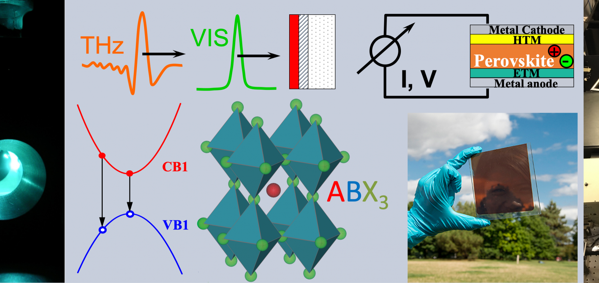

Optically Determined Hole Effective Mass in Tin-Iodide Perovskite Films
ACS Energy Letters American Chemical Society 10:9 (2025) 4589-4595
Abstract:
Tin-halide perovskites currently offer the best photovoltaic performance of lead-free metal-halide semiconductors. However, their transport properties are mostly dominated by holes, owing to ubiquitous self-doping. Here we demonstrate a noncontact, optical spectroscopic method to determine the effective mass of the dominant hole species in FASnI3, by investigating a series of thin films with hole densities finely tuned through either SnF2 additive concentration or controlled exposure to air. We accurately determine the plasma frequency from mid-infrared reflectance spectra by modeling changes in the vibrational response of the FA cation as the plasma edge shifts through the molecular resonance. Our approach yields a hole effective mass of 0.28m e for FASnI3 and demonstrates parabolicity within ∼100 meV of the valence band edge. An absence of Fano contributions further highlights insignificant coupling between the hole plasma and FA cation. Overall, this approach enables noncontact screening of thin-film materials for optimized charge-carrier transport properties.Highly Crystalline and Oriented Thin Films of Fully Conjugated 3D‐Covalent Organic Frameworks
Angewandte Chemie International Edition Wiley (2025) e202505799
Abstract:
Fully conjugated 3D covalent organic frameworks (COFs) are a newly emerged class of materials that expands reticular chemistry to extended electron delocalization for optoelectronic applications. To overcome the limitations of sp3‐connected 3D frameworks, the pseudo‐tetrahedral motif cyclooctatetrathiophene (COTh) has gained attention for forming fully conjugated 3D COFs. We report on a novel COTh building block, featuring functional formyl groups directly attached to the core's conjugated thiophenes. The modulation synthesis approach with mono‐functionalized inhibitors enables the formation of COTh‐1P COF, which exhibited remarkable crystallinity and permanent porosity. By following this approach and by optimizing the synthesis conditions for the solvothermal growth of thin films, we fabricated the first preferentially oriented conjugated 3D COF films on various substrates without pre‐functionalization. With these thin films, optical pump terahertz probe studies allowed us, for the first time with 3D‐fully conjugated COFs, to provide insights into the excited state and charge‐carrier dynamics of these unique organic frameworks. Low effective masses are discovered for valence and conduction bands by density functional theory simulations. The ability to create crystalline and oriented films of fully π‐conjugated 3D COTh‐based COFs on non‐modified substrates is expected to open the way for integration of such frameworks into diverse optoelectronic applications.Impact of Charge Transport Layers on the Structural and Optoelectronic Properties of Coevaporated Cu 2 AgBiI 6
ACS Applied Materials & Interfaces American Chemical Society 17:28 (2025) 40363-40374
Abstract:
The copper–silver–bismuth–iodide compound Cu2AgBiI6 has emerged as a promising lead-free and environmentally friendly alternative to wide-bandgap lead-halide perovskites for applications in multijunction solar cells. Despite its promising optoelectronic properties, the efficiency of Cu2AgBiI6 is still severely limited by poor charge collection. Here, we investigate the impact of commonly used charge transport layers (CTLs), including poly[bis(4-phenyl)(2,4,6-trimethylphenyl)amine] (PTAA), CuI, [6,6]-phenyl-C61-butyric acid methyl ester (PCBM), and SnO2, on the structural and optoelectronic properties of coevaporated Cu2AgBiI6 thin films. We reveal that while organic transport layers, such as PTAA and PCBM, form a relatively benign interface, inorganic transport layers, such as CuI and SnO2, induce the formation of unintended impurity phases within the CuI–AgI–BiI3 solid solution space, significantly influencing structural and optoelectronic properties. We demonstrate that identification of these impurity phases requires careful cross-validation combining absorption, X-ray diffraction and THz photoconductivity spectroscopy because their structural and optoelectronic properties are very similar to those of Cu2AgBiI6. Our findings highlight the critical role of CTLs in determining the structural and optoelectronic properties of coevaporated copper–silver–bismuth–iodide thin films and underscore the need for advanced interface engineering to optimize device efficiency and reproducibility.Ultrafast Nanoscopy of Carrier Dynamics and Nanoscale Morphology in Metal Halide Perovskites
Institute of Electrical and Electronics Engineers (IEEE) 00 (2025) 1-1
Abstract:
The rise of metal halide perovskites has prompted a revolution in optoelectronics research [1]. Yet a comprehensive understanding of the vertical charge transport that underlies the soaring efficiencies of perovskite-based solar cells has remained challenging owing to the materials' nanocrystalline structure [2] and competing crystal phases [3]. Here, we simultaneously probe the intrinsic out-of-plane charge-carrier diffusion and the nanoscale morphology by pushing depth-sensitive terahertz near- field nano-spectroscopy [4] to extreme subcycle timescales [5]. Evanescent terahertz fields at the apex of a metallic tip probe ultrafast dynamics of photocarriers in $\text{FA}_{0}.{}_{83}\text{Cs}_{0.17}\text{Pb}(\mathrm{I}_{1}{}_{-\mathrm{x}}\mathrm{C}1_{\mathrm{x}})_{3}$ films with nanoscale spatial resolution (Fig. 1 a). By analysing characteristic phonon signatures in the spectral response, we distinguish domains of the photo active cubic $\alpha$ -phase from the trigonal δ-phase and $\text{PbI}_{2}$ nano-islands (Fig. 1 b). To examine the impact of these nanoscale inhomogeneities on carrier dynamics, we monitor the peak pump-induced signal as a function of pump delay time $t_{\mathrm{p}}$ (Fig. 1c). Notably, the full pump-induced waveforms at different $t_{\mathrm{p}}$ (Fig. 1d) show a deeply subcycle time shift $\Delta t$, which can be microscopically linked to a diffusion-driven change in the vertical carrier distribution with $t_{\mathrm{r}}$ (Fig. 1e, inset). Com-bining a straightforward rate equation model with the finite-dipole model, we extract the evolution of the out-of-plane carrier density profile from $\Delta t$ (Fig. 1e). Mapping the out-of-plane diffusion coefficient $D$ along a line across different grains, including $\alpha$ -phase grains and $\text{PbI}_{2}$ contaminations, we find a homogeneous value of $D=(0.2\pm 0.1)\ \text{cm}^{2}\mathrm{s}^{-1}$, which is surprisingly immune to compositional and structural variations (Fig. 1 f). This robustness of vertical diffusion may contribute to the exceptional performance of perovskite-based devices. Linking in situ carrier transport with nanoscale morphology and chemical composition could introduce a paradigm shift for the analysis and optimization of next-generation optoelectronics that are based on nanocrystalline materials.Ruddlesden–Popper Defects Act as a Free Surface: Role in Formation and Photophysical Properties of CsPbI 3
Advanced Materials Wiley (2025) 2501788