Solution-Processed All-Perovskite Multi-junction Solar Cells
Joule 3:2 (2019) 387-401
Authors:
DP McMeekin, S Mahesh, NK Noel, MT Klug, JC Lim, JH Warby, JM Ball, LM Herz, MB Johnston, HJ Snaith
Abstract:
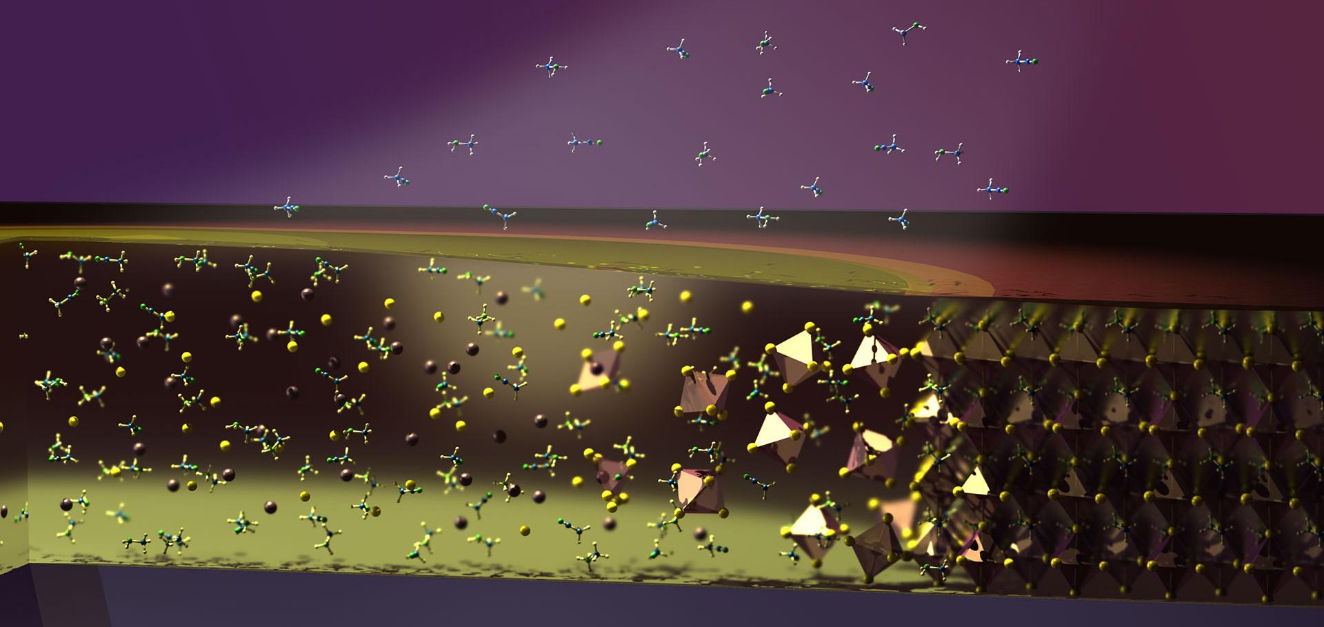
© 2019 Multi-junction device architectures can increase the power conversion efficiency (PCE) of photovoltaic (PV) cells beyond the single-junction thermodynamic limit. However, these devices are challenging to produce by solution-based methods, where dissolution of underlying layers is problematic. By employing a highly volatile acetonitrile(CH 3 CN)/methylamine(CH 3 NH 2 ) (ACN/MA) solvent-based perovskite solution, we demonstrate fully solution-processed absorber, transport, and recombination layers for monolithic all-perovskite tandem and triple-junction solar cells. By combining FA 0.83 Cs 0.17 Pb(Br 0.7 I 0.3 ) 3 (1.94 eV) and MAPbI 3 (1.57 eV) junctions, we reach two-terminal tandem PCEs of more than 15% (steady state). We show that a MAPb 0.75 Sn 0.25 I 3 (1.34 eV) narrow band-gap perovskite can be processed via the ACN/MA solvent-based system, demonstrating the first proof-of-concept, monolithic all-perovskite triple-junction solar cell with an open-circuit voltage reaching 2.83 V. Through optical and electronic modeling, we estimate the achievable PCE of a state-of-the-art triple-junction device architecture to be 26.7%. Our work opens new possibilities for large-scale, low-cost, printable perovskite multi-junction solar cells. Silicon-based solar cells are dominating today's solar energy market. However, their efficiencies will soon reach their maximum practical limit. Without any gains in efficiency, price reductions will become increasingly difficult to achieve. Tandem and multi-junction architectures can overcome this single-junction efficiency limit. Perovskite materials offer both band-gap tunability and solution processability. This unique combination of properties allows for fabrication of multi-junction solar cells using high-throughput deposition techniques such as blade coating, roll-to-roll, gravure coating or inkjet printing. However, these solar cells have yet to be fabricated using these deposition techniques due to difficulties in sequentially depositing these semiconductors. By utilizing an acetonitrile/methylamine-based solvent, we demonstrate the first monolithic all-perovskite multi-junction solar cells fabricated via solution processing of all active layers, apart from the electrodes. Perovskite solar cells can be processed using solution-based methods. Furthermore, perovskite solar cells can tune their band gap to absorb different portions of the solar spectrum. This property allows for fabrication of multi-junction solar cell, which can offer higher power conversion efficiencies than single-junction architecture. Here, we combine both features to fabricate the first solution-processed, monolithic, all-perovskite tandem and triple-junction solar cells.