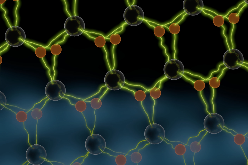
A layered view of NbSe2 showing the crystal lattice (top), the symmetry-pinned orbital cloud at empty sites (middle), and the STM image (bottom) that directly reveals this hidden electronic structure.
An international team led by a researcher at the University of Oxford has obtained the first direct experimental evidence of a rare electronic state – known as an obstructed atomic band – in a two-dimensional quantum material. The findings, published in Nature Physics, open new avenues for understanding and designing quantum materials, with potential implications for catalysis and superconductivity.
In most crystalline materials, electrons cluster around atomic nuclei, as one might expect. But in a certain class of materials, something more surprising occurs: the electrons instead gather at empty points in the crystal lattice – gaps between the atoms rather than the atoms themselves. This phenomenon, known as an obstructed atomic band, is not a quirk of geometry but a robust signature of the interplay between symmetry and topology in the material's electronic structure.
Until now, the existence of such bands had only been proposed theoretically, with indirect experimental hints at best. In the new study, researchers achieved a direct and unambiguous identification of an obstructed atomic band in NbSe₂ which is a layered material made of niobium and selenium that also becomes superconducting at low temperatures.
Dr Dumitru Călugăru, a Leverhulme-Peierls Fellow in the Department of Physics at the University of Oxford and lead author of the study, explains: 'Up to now, multiple materials have been proposed as hosting obstructed atomic bands, and some studies did provide indirect experimental evidence that such bands could exist. However, a direct and unambiguous identification of such a band has been lacking.'
To achieve this, the team used scanning tunnelling microscopy (STM) which is a technique capable of imaging the electronic structure of a material at the atomic scale. A key insight was turning an apparent disadvantage into an asset: rather than seeking a perfectly pure crystal, the researchers exploited a minute concentration of natural impurities to pinpoint the positions of the atomic nuclei in their images which would otherwise have been invisible. By combining these STM images with first-principles calculations, the team established that the electron wave functions interfere in such a way that the centre of mass of the electron density distribution lies at an empty point in the lattice thus providing direct confirmation of the obstructed atomic band.
The result raises new questions about NbSe₂ itself. The material is well known for its superconducting properties and for developing a charge-density wave – a periodic modulation of electron density – and the discovery opens the question of whether the obstructed atomic band influences, or perhaps even helps drive, these transitions. Beyond NbSe₂, the work introduces a broadly applicable methodology, allowing maps of electron wave functions to be connected directly to detailed theoretical descriptions of electronic states; it is a tool that could be applied across a wide range of quantum materials, including those whose microscopic description remains poorly understood.
The findings may also have practical consequences. Because the empty lattice sites where the electrons gather are unoccupied by atomic nuclei, they present natural candidates for active catalytic sites. 'The empty sites where the orbitals of the obstructed bands are located are natural candidates for active catalytic sites, because they host a large density of electronic states, but no atomic nucleus to get in the way of the reactants,' adds Dr Călugăru.
More broadly, this work bridges the gap between abstract band theory and real-space intuition by directly imaging electronic wave functions. Such an approach opens a path to uncovering hidden electronic structure in quantum materials and guiding the design of new ones where topology and functionality go hand in hand.
Observation of an obstructed atomic band in a transition metal dichalcogenide, D Călugăru et al., Nature Physics (2026)