In quantum computing building two-dimensional (2D) lattices of hundreds or thousands of individually addressable, highly coherent qubits is an outstanding hardware challenge. Anticipated applications include demonstrations of logic gates using the surface code and quantum simulations of 2D lattice Hamiltonians. Superconducting circuits are a promising platform for realising such lattices; qubits are lithographically defined on 2D substrates, and tailored coupling circuitry can be included in the regions between qubits to realise a universal gate set. Two requirements for scaling such superconducting qubit lattices are: firstly, a method to route control wiring to the circuit such that all qubits remain addressable and measurable at progressively larger scales and secondly, a means of preventing low frequency spurious modes from emerging in the circuit as the dimensions increase.
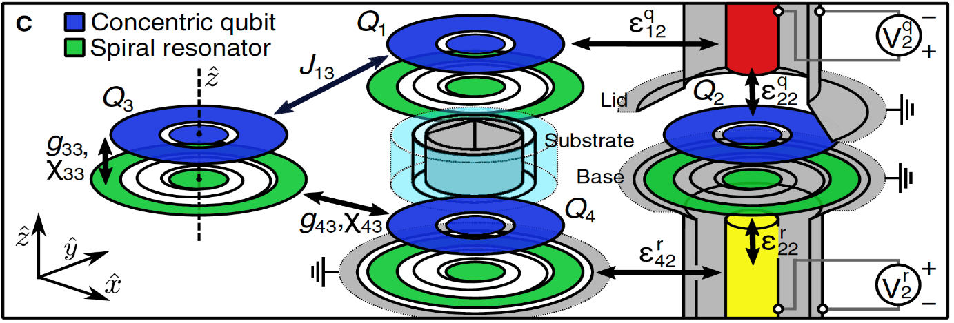
Peter Spring in Dr Peter Leek’s group and his co-workers have published work in Science Advances (http://dx.doi.org/10.1126/sciadv.abl6698) that reports on high qubit coherence as well as low cross-talk and single-qubit gate errors in a superconducting circuit architecture that promises to be tileable to two-dimensional (2D) lattices of qubits. The proof-of-principle device features four uncoupled transmon qubits and exhibits average energy relaxation times T1 = 149(38) μs, pure echoed dephasing times T𝜙,e =189(34) μs, and single-qubit gate fidelities F = 99.982(4)% as measured by simultaneous randomised benchmarking. The 3D integrated nature of the control wiring means that qubits will remain addressable as the architecture is tiled to form larger qubit lattices.