Home
Department Of Physics text logo
  • Research
    • Our research
    • Our research groups
    • Our research in action
    • Research funding support
    • Summer internships for undergraduates
  • Study
    • Undergraduates
    • Postgraduates
  • Engage
    • For alumni
    • For business
    • For schools
    • For the public
Menu
CMP
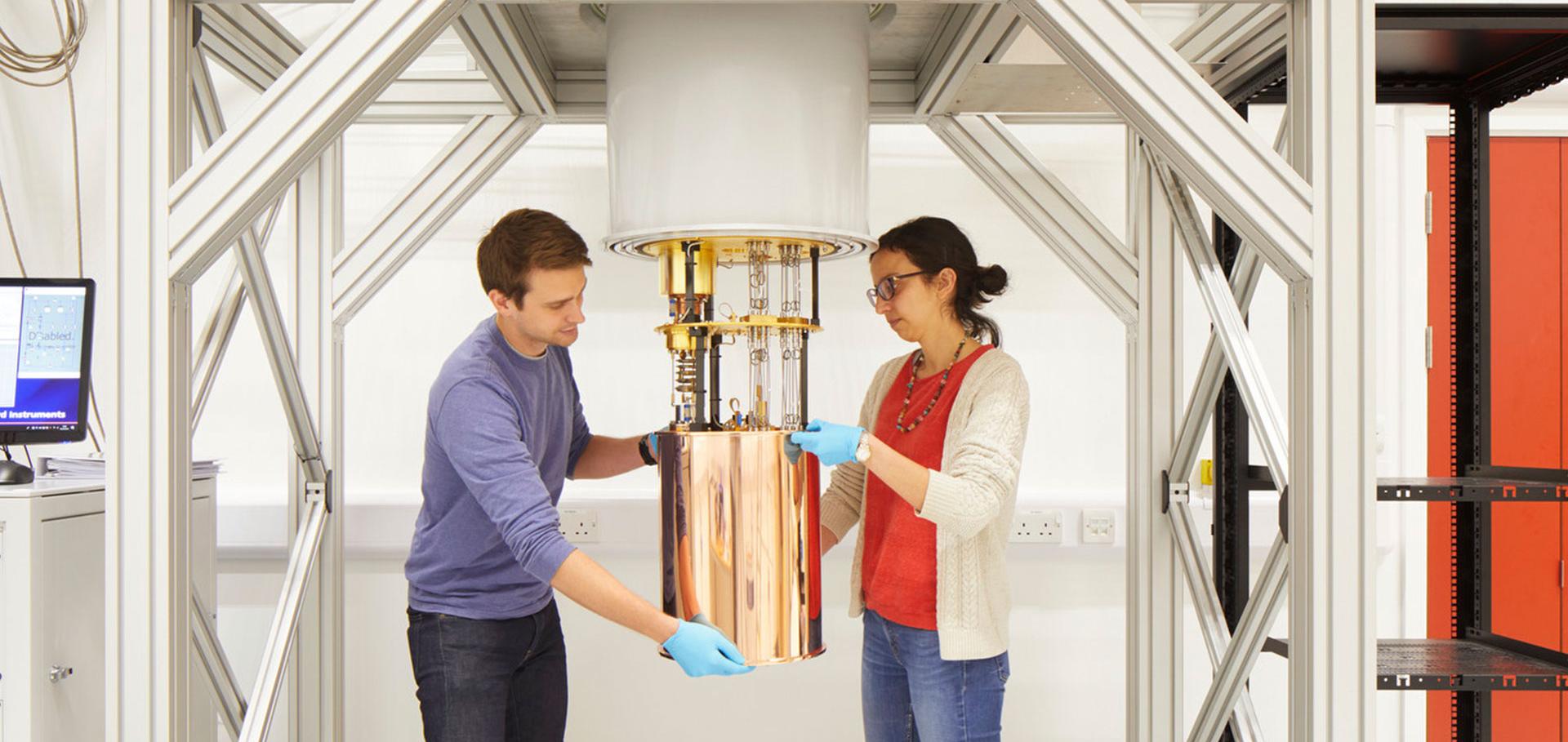
Credit: Jack Hobhouse

Prof Henry Snaith FRS

Professor of Physics

Sub department

  • Condensed Matter Physics

Research groups

  • Snaith group
  • Advanced Device Concepts for Next-Generation Photovoltaics
Henry.Snaith@physics.ox.ac.uk
Robert Hooke Building, room G21
  • About
  • Publications

Impact of hole-transport layer and interface passivation on halide segregation in mixed-halide perovskites

Advanced Functional Materials Wiley 32:41 (2022) 2204825

Authors:

Vincent JY Lim, Alexander J Knight, Robert DJ Oliver, Henry J Snaith, Michael B Johnston, Laura M Herz

Abstract:

Mixed-halide perovskites offer ideal bandgaps for tandem solar cells, but photoinduced halide segregation compromises photovoltaic device performance. This study explores the influence of a hole-transport layer, necessary for a full device, by monitoring halide segregation through in situ, concurrent X-ray diffraction and photoluminescence measurements to disentangle compositional and optoelectronic changes. This work demonstrates that top coating FA0.83Cs0.17Pb(Br0.4I0.6)3 perovskite films with a poly(triaryl)amine (PTAA) hole-extraction layer surprisingly leads to suppression of halide segregation because photogenerated charge carriers are rapidly trapped at interfacial defects that do not drive halide segregation. However, the generation of iodide-enriched regions near the perovskite/PTAA interface enhances hole back-transfer from the PTAA layer through improved energy level offsets, increasing radiative recombination losses. It is further found that while passivation with a piperidinium salt slows halide segregation in perovskite films, the addition of a PTAA top-coating accelerates such effects, elucidating the specific nature of trap types that are able to drive the halide segregation process. This work highlights the importance of selective passivation techniques for achieving efficient and stable wide-bandgap perovskite photovoltaic devices.
More details from the publisher
Details from ORA
More details

In Operando, Photovoltaic, and Microscopic Evaluation of Recombination Centers in Halide Perovskite-Based Solar Cells.

ACS applied materials & interfaces 14:30 (2022) 34171-34179

Authors:

Arava Zohar, Michael Kulbak, Silver H Turren-Cruz, Pabitra K Nayak, Adi Kama, Anders Hagfeldt, Henry J Snaith, Gary Hodes, David Cahen

Abstract:

The origin of the low densities of electrically active defects in Pb halide perovskite (HaP), a crucial factor for their use in photovoltaics, light emission, and radiation detection, remains a matter of discussion, in part because of the difficulty in determining these densities. Here, we present a powerful approach to assess the defect densities, based on electric field mapping in working HaP-based solar cells. The minority carrier diffusion lengths were deduced from the electric field profile, measured by electron beam-induced current (EBIC). The EBIC method was used earlier to get the first direct evidence for the n-i-p junction structure, at the heart of efficient HaP-based PV cells, and later by us and others for further HaP studies. This manuscript includes EBIC results on illuminated cell cross sections (in operando) at several light intensities to compare optoelectronic characteristics of different cells made by different groups in several laboratories. We then apply a simple, effective single-level defect model that allows deriving the densities (Nr) of the defect acting as recombination center. We find Nr ≈ 1 × 1013 cm-3 for mixed A cation lead bromide-based HaP films and ∼1 × 1014 cm-3 for MAPbBr3(Cl). As EBIC photocurrents are similar at the grain bulk and boundaries, we suggest that the defects are at the interfaces with selective contacts rather than in the HaP film. These results are relevant for photovoltaic devices as the EBIC responses distinguish clearly between high- and low-efficiency devices. The most efficient devices have n-i-p structures with a close-to-intrinsic HaP film, and the selective contacts then dictate the electric field strength throughout the HaP absorber.
More details from the publisher
More details
More details

Rapid sequestration of perovskite solar cell-derived lead in soil.

Journal of hazardous materials 436 (2022) 128995

Authors:

Felix Schmidt, Luca Ledermann, Andreas Schäffer, Henry J Snaith, Markus Lenz

Abstract:

Efficient and stable perovskite solar cells rely on the use of Pb species potentially challenging the technologies' commercialisation. In this study, the fate of Pb derived from two common perovskite precursors is compared to cationic lead in soil-water microcosm experiments under various biogeochemical conditions. The rapid and efficient removal of Pb from the aqueous phase is demonstrated by inductively coupled plasma mass spectrometry. Sequential soil extraction results reveal that a substantial amount of Pb is associated with immobile fractions, whereas a minor proportion of Pb may become available again in the long term, when oxygen is depleted (e.g. during water logging). X-ray absorption spectroscopy results reveal that the sorption of Pb on mineral phases represents the most likely sequestration mechanism. The obtained results suggest that the availability of leached Pb from perovskite solar cells is naturally limited in soils and that its adverse effects on soil biota are possibly negligible in oxic soils. All three Pb sources used behaved very similar in the experiments, wherefore we conclude that perovskite derived Pb will have a similar fate compared to cationic Pb, so that established risk assessment considerations for Pb remain legitimate.
More details from the publisher
More details
More details

Long-range charge carrier mobility in metal halide perovskite thin-films and single crystals via transient photo-conductivity

Nature Communications Springer Nature 13:1 (2022) 4201

Authors:

Jongchul Lim, Manuel Kober-Czerny, Yen-Hung Lin, James M Ball, Nobuya Sakai, Elisabeth A Duijnstee, Min Ji Hong, John G Labram, Bernard Wenger, Henry J Snaith

Abstract:

Charge carrier mobility is a fundamental property of semiconductor materials that governs many electronic device characteristics. For metal halide perovskites, a wide range of charge carrier mobilities have been reported using different techniques. Mobilities are often estimated via transient methods assuming an initial charge carrier population after pulsed photoexcitation and measurement of photoconductivity via non-contact or contact techniques. For nanosecond to millisecond transient methods, early-time recombination and exciton-to-free-carrier ratio hinder accurate determination of free-carrier population after photoexcitation. By considering both effects, we estimate long-range charge carrier mobilities over a wide range of photoexcitation densities via transient photoconductivity measurements. We determine long-range mobilities for FA0.83Cs0.17Pb(I0.9Br0.1)3, (FA0.83MA0.17)0.95Cs0.05Pb(I0.9Br0.1)3 and CH3NH3PbI3-xClx polycrystalline films in the range of 0.3 to 6.7 cm2 V−1 s−1. We demonstrate how our data-processing technique can also reveal more precise mobility estimates from non-contact time-resolved microwave conductivity measurements. Importantly, our results indicate that the processing of polycrystalline films significantly affects their long-range mobility.
More details from the publisher
Details from ORA
More details
More details

Understanding and Minimizing $V_{OC}$ Losses in All-Perovskite Tandem Photovoltaics

(2022)

Authors:

Jarla Thiesbrummel, Francisco Peña-Camargo, Kai Oliver Brinkmann, Emilio Gutierrez-Partida, Fengjiu Yang, Jonathan Warby, Steve Albrecht, Dieter Neher, Thomas Riedl, Henry J Snaith, Martin Stolterfoht, Felix Lang
More details from the publisher
Details from ArXiV

Pagination

  • First page First
  • Previous page Prev
  • …
  • Page 18
  • Page 19
  • Page 20
  • Page 21
  • Current page 22
  • Page 23
  • Page 24
  • Page 25
  • Page 26
  • …
  • Next page Next
  • Last page Last

Footer Menu

  • Contact us
  • Giving to the Dept of Physics
  • Work with us
  • Media

User account menu

  • Log in

Follow us

FIND US

Clarendon Laboratory,

Parks Road,

Oxford,

OX1 3PU

CONTACT US

Tel: +44(0)1865272200

University of Oxfrod logo Department Of Physics text logo
IOP Juno Champion logo Athena Swan Silver Award logo

© University of Oxford - Department of Physics

Cookies | Privacy policy | Accessibility statement

Built by: Versantus

  • Home
  • Research
  • Study
  • Engage
  • Our people
  • News & Comment
  • Events
  • Our facilities & services
  • About us
  • Current students
  • Staff intranet