Home
Department Of Physics text logo
  • Research
    • Our research
    • Our research groups
    • Our research in action
    • Research funding support
    • Summer internships for undergraduates
  • Study
    • Undergraduates
    • Postgraduates
  • Engage
    • For alumni
    • For business
    • For schools
    • For the public
Menu
CMP
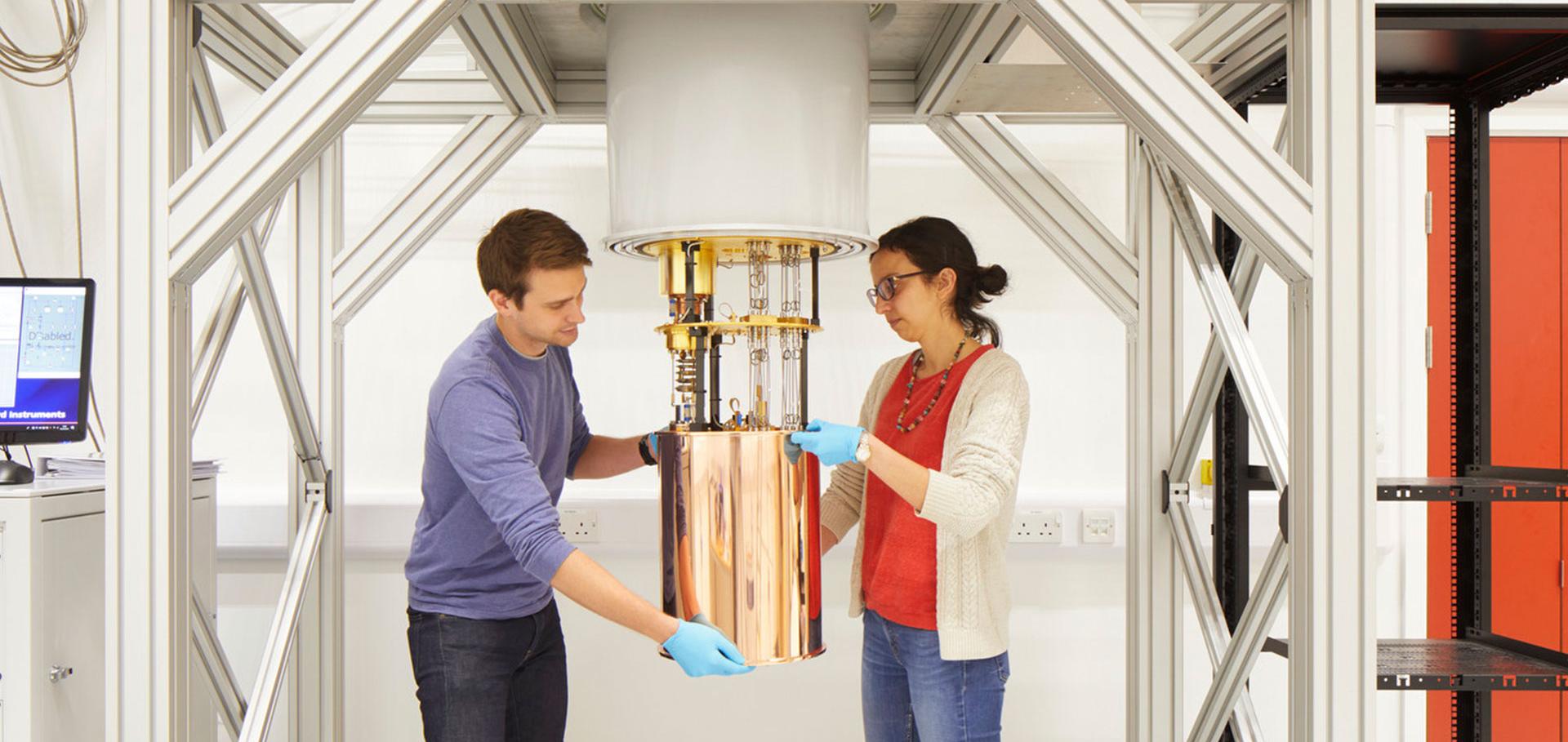
Credit: Jack Hobhouse

Prof Henry Snaith FRS

Professor of Physics

Sub department

  • Condensed Matter Physics

Research groups

  • Snaith group
  • Advanced Device Concepts for Next-Generation Photovoltaics
Henry.Snaith@physics.ox.ac.uk
Robert Hooke Building, room G21
  • About
  • Publications

Disentangling degradation pathways of narrow bandgap lead-tin perovskite material and photovoltaic devices.

Nature communications 16:1 (2025) 5450

Authors:

Florine M Rombach, Akash Dasgupta, Manuel Kober-Czerny, Heon Jin, James M Ball, Joel A Smith, Michael D Farrar, Henry J Snaith

Abstract:

Narrow bandgap lead-tin perovskites are essential components of next-generation all-perovskite multi-junction solar cells. However, their poor stability under operating conditions hinders successful implementation. In this work, we systematically investigate the underlying mechanisms of this instability under combined heat and light stress (ISOS L-2 conditions) by measuring changes in phase, conductivity, recombination and current-voltage characteristics. We find an increased impact of the redistribution of mobile ions during device operation to be the primary driver of performance loss during stressing, with further losses caused by a slower increase in non-radiative recombination and background hole density. Crucially, the dominant degradation mode changes with different hole transport materials, which we attribute to variations in iodine vacancy generation rates. By quantifying the impact of these mechanisms on device performance, we provide critical insights for improving the operational stability of lead-tin perovskite solar cells.
More details from the publisher
More details

Impact of Charge Transport Layers on the Structural and Optoelectronic Properties of Coevaporated Cu<sub>2</sub>AgBiI<sub>6</sub>.

ACS applied materials & interfaces (2025)

Authors:

Jae Eun Lee, Marcello Righetto, Benjamin WJ Putland, Siyu Yan, Joshua RS Lilly, Snigdha Lal, Heon Jin, Nakita K Noel, Michael B Johnston, Henry J Snaith, Laura M Herz

Abstract:

The copper-silver-bismuth-iodide compound Cu2AgBiI6 has emerged as a promising lead-free and environmentally friendly alternative to wide-bandgap lead-halide perovskites for applications in multijunction solar cells. Despite its promising optoelectronic properties, the efficiency of Cu2AgBiI6 is still severely limited by poor charge collection. Here, we investigate the impact of commonly used charge transport layers (CTLs), including poly[bis(4-phenyl)(2,4,6-trimethylphenyl)amine] (PTAA), CuI, [6,6]-phenyl-C61-butyric acid methyl ester (PCBM), and SnO2, on the structural and optoelectronic properties of coevaporated Cu2AgBiI6 thin films. We reveal that while organic transport layers, such as PTAA and PCBM, form a relatively benign interface, inorganic transport layers, such as CuI and SnO2, induce the formation of unintended impurity phases within the CuI-AgI-BiI3 solid solution space, significantly influencing structural and optoelectronic properties. We demonstrate that identification of these impurity phases requires careful cross-validation combining absorption, X-ray diffraction and THz photoconductivity spectroscopy because their structural and optoelectronic properties are very similar to those of Cu2AgBiI6. Our findings highlight the critical role of CTLs in determining the structural and optoelectronic properties of coevaporated copper-silver-bismuth-iodide thin films and underscore the need for advanced interface engineering to optimize device efficiency and reproducibility.
More details from the publisher
More details

Present status of and future opportunities for all-perovskite tandem photovoltaics

Nature Energy Springer Nature (2025) 1-16

Authors:

Jin Wen, Hang Hu, Chao Chen, David P McMeekin, Ke Xiao, Renxing Lin, Ye Liu, Henry J Snaith, Jiang Tang, Ulrich W Paetzold, Hairen Tan
More details from the publisher
More details

Diamine surface passivation and postannealing enhance the performance of silicon-perovskite tandem solar cells

ACS Applied Materials & Interfaces American Chemical Society (2025)

Authors:

Margherita Taddei, Hannah Contreras, Hai-Nam Doan, Declan P McCarthy, Seongrok Seo, Robert JE Westbrook, Daniel J Graham, Kunal Datta, Perrine Carroy, Delfina Muñoz, Juan-Pablo Correa-Baena, Stephen Barlow, Seth R Marder, Joel A Smith, Henry Snaith, David S Ginger

Abstract:

We show that the use of 1,3-diaminopropane (DAP) as a chemical modifier at the perovskite/electron-transport layer (ETL) interface enhances the power conversion efficiency (PCE) of 1.7 eV band gap mixed-halide perovskite containing formamidinium and Cs single-junction cells, primarily by increasing the open-circuit voltage (VOC) from 1.06 to 1.15 V. We find that adding a postprocessing annealing step after C60 evaporation further improves device performance. Specifically, the fill factor (FF) increases by 20% in the DAP + postannealing devices compared to the control. Using hyperspectral photoluminescence microscopy, we demonstrate that annealing helps improve compositional homogeneity at the electron-transport layer (ETL) and hole-transport layer (HTL) interfaces of the solar cell, which prevents detrimental band gap pinning in the devices and improves C60 adhesion. Using time-of-flight secondary ion mass spectrometry, we show that DAP reacts with formamidinium (FA+) present at the surface of the perovskite structure to form a larger molecular cation, 1,4,5,6-tetrahydropyrimidinium (THP+), which remains at the interface. Combining the use of DAP and annealing the C60 interface, we fabricate Si-perovskite tandems with a PCE of 25.29%, compared to 23.26% for control devices. Our study underscores the critical role of the chemical reactivity of diamines at the surface and the thermal postprocessing of the C60/Lewis-base passivator interface in minimizing device losses and enhancing solar-cell performance of wide-band-gap mixed-cation mixed-halide perovskites for tandem applications.
More details from the publisher
Details from ORA
More details

Indium and Silver Recovery from Perovskite Thin Film Solar Cell Waste by Means of Nanofiltration.

ACS sustainable resource management 2:6 (2025) 1087-1095

Authors:

Meret Amrein, Karina Rohrer, Dirk Hengevoss, Heon Jin, Henry J Snaith, Michael Thomann, Frank Nüesch, Markus Lenz

Abstract:

Due to minimal material use and low-cost processing, next-generation thin film solar cells represent a promising alternative to traditional crystalline silicon solar cells. Among these, metal-halide perovskite solar cells have seen significant improvements in power conversion efficiency and are now on the verge of market entry. However, most efficient and stable perovskite solar cells contain lead in the perovskite absorber layer, along with indium and silver in their electrodes. This study demonstrates an environmentally benign recycling process for recovering all three elements from end-of-life perovskite solar cells. In short, the process consists of mechanical dismantling (milling), aqueous extraction/purification of PbI2, and acid extraction and purification of indium and silver by nanofiltration. After the quantitative recovery of lead as PbI2 (95 ± 5%), indium and silver were dissolved using nitric acid with recovery rates of 87 ± 7% for both metals. Life cycle assessment calculations were used to determine optimal conditions in terms of minimal environmental impact per gram of extracted element. After acid extraction, nanofiltration was employed using both custom-made layer-by-layer membranes and commercially available acid-resistant flat sheet membranes to separate indium from silver. Using an optimized membrane design, indium was almost entirely retained (96.9 ± 0.4%) using a layer-by-layer membrane at 50% permeate recovery. Hence, a twofold concentration of indium was achieved over the course of the filtration. In contrast, silver was not retained (retention of -7.6 ± 6.3%), resulting in a dilute Ag permeate. Using the commercial flat sheet membrane resulted in similar retention rates, with 98.5 ± 0.4% for indium and 5.8 ± 11.6% for silver. However, this came at the expense of considerably higher operating pressure (25 bar vs 5 bar) and lower flux (6 L/m2h vs 30 L/m2h), resulting in higher energy demand (72 Wh/L vs 9 Wh/L). Therefore, layer-by-layer membrane filtration proved to be the superior method for element recovery from perovskite photovoltaic devices. This study has shown that combining hydrometallurgical processing (aqueous and acidic extraction) with layer-by-layer membrane filtration offers an efficient and environmentally benign approach for metal recovery from end-of-life solar cells. Since indium and silver are also key elements for other thin film photovoltaic applications, layer-by-layer membrane filtration may represent a platform technology for future photovoltaic panel recycling.
More details from the publisher

Pagination

  • Current page 1
  • Page 2
  • Page 3
  • Page 4
  • Page 5
  • Page 6
  • Page 7
  • Page 8
  • Page 9
  • …
  • Next page Next
  • Last page Last

Footer Menu

  • Contact us
  • Giving to the Dept of Physics
  • Work with us
  • Media

User account menu

  • Log in

Follow us

FIND US

Clarendon Laboratory,

Parks Road,

Oxford,

OX1 3PU

CONTACT US

Tel: +44(0)1865272200

University of Oxfrod logo Department Of Physics text logo
IOP Juno Champion logo Athena Swan Silver Award logo

© University of Oxford - Department of Physics

Cookies | Privacy policy | Accessibility statement

Built by: Versantus

  • Home
  • Research
  • Study
  • Engage
  • Our people
  • News & Comment
  • Events
  • Our facilities & services
  • About us
  • Current students
  • Staff intranet