Investigation of luminescence and scintillation properties of a ZnS-Ag/6LiF scintillator in the 7-295 K temperature range
Journal of Luminescence 134 (2013) 63-66
Abstract:
The luminescence and scintillation properties of ZnS-Ag/6LiF where studied in the 7-295 K temperature range to evaluate the suitability of the scintillator for neutron detection at very low temperature (<1 K). It is shown that decrease of temperature has little effect upon principal luminescence and scintillation characteristics of ZnS-Ag: the changes of emission intensity are small for photoexcitation and negligible for excitation with α-particles. The recombination kinetics of the scintillation decay exhibits modest shortening of the fast decay time constant, from 4.52 to 3.35 μs with cooling to 10 K. It is concluded that ZnS-Ag/6LiF is a promising scintillator for cryogenic application. © 2012 Elsevier B.V. All rights reserved.Optimization of light collection from crystal scintillators for cryogenic experiments
4th International Conference on Current Problems in Nuclear Physics and Atomic Energy, NPAE 2012 - Proceedings (2013) 400-403
Abstract:
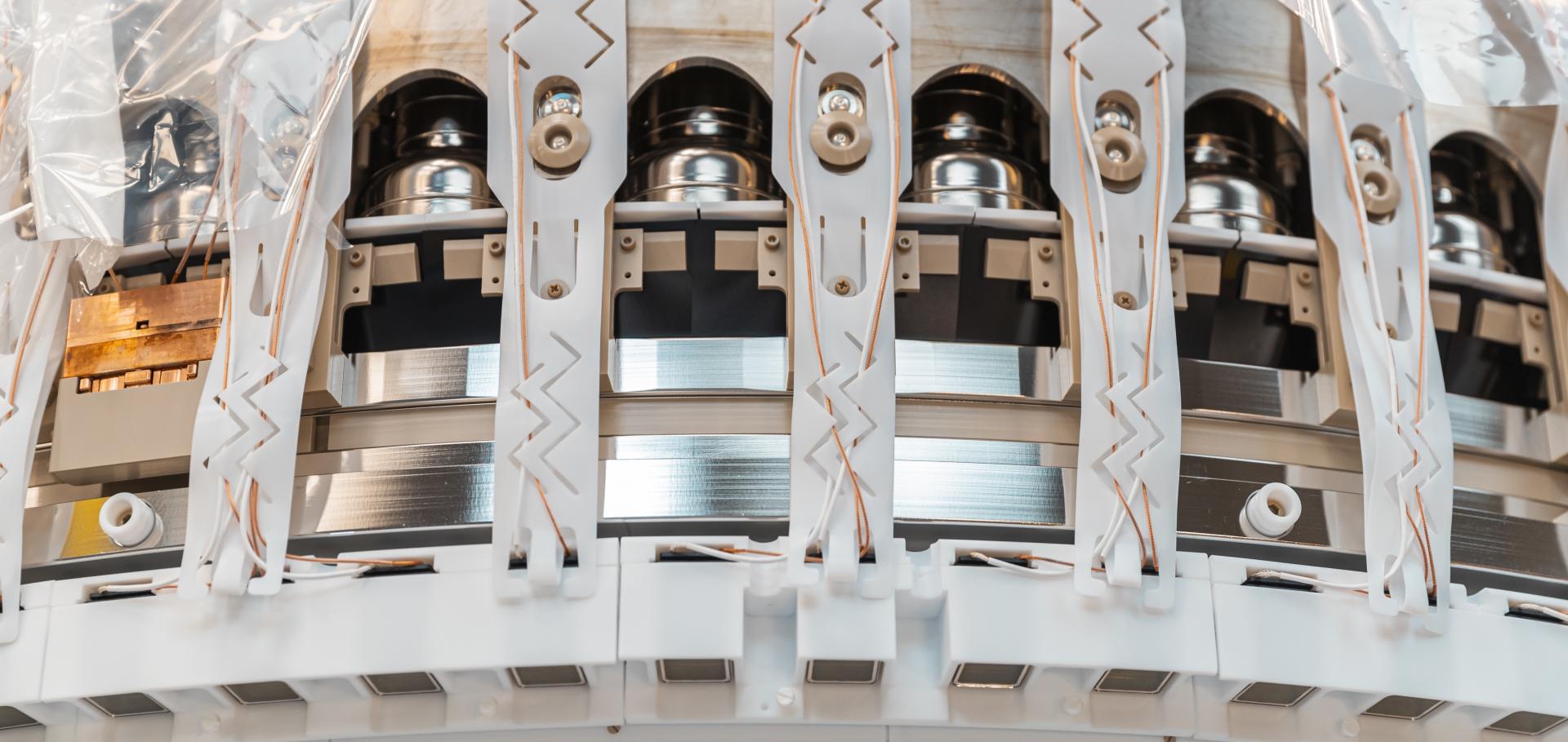
Cryogenic scintillation bolometers are a promising technique to search for dark matter and neutrinoless double β decay. Improvement of light collection and energy resolution are important requirements in such experiments. Energy resolutions and relative pulse amplitudes of scintillation detectors using ZnWO4 scintillation crystals of different shapes (cylinder Ø 20 × 20 mm and hexagonal prism with diagonal 20 mm and height 20 mm), reflector materials and shapes, optical contact and surface properties (polished and diffused) were measured. The crystal scintillator of hexagonal shape shows the better energy resolution and pulse amplitude. The best energy resolution (FWHM = 9.3 % for 662 keV γ quanta of 137Cs) was obtained with a hexagonal scintillator with all surfaces diffuse, in optical contact with a PMT and surrounded by a reflector (3M) of size Ø 26 × 25 mm. In the geometry "without optical contact" representing the conditions of light collection for a cryogenic scintillating bolometer the best energy resolution and relative pulse amplitude was obtained for a hexagonal shape scintillator with diffuse side and polished face surfaces, surrounded by a reflector with a gap between the scintillator and the reflector.Axion searches with the EDELWEISS-II experiment
JOURNAL OF COSMOLOGY AND ASTROPARTICLE PHYSICS (2013) ARTN 067
Development of techniques for characterisation of scintillation materials for cryogenic application
Radiation Measurements (2013)
Search for low-mass WIMPs with EDELWEISS-II heat-and-ionization detectors
Physical Review D - Particles, Fields, Gravitation and Cosmology 86:5 (2012)