
Topological materials for helicity-dependent THz emission
Abstract:
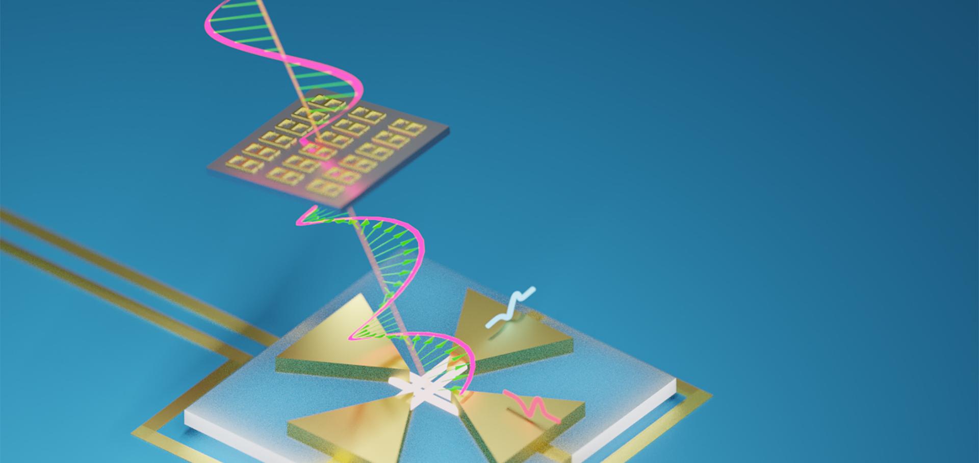
Topological insulator (TI) materials are emerging as novel materials for spintronic applications. Here, we demonstrate helicity-dependent THz emission from Dirac semi-metal Cd 3 As 2 nanowires and used scattering-type scanning optical microscopy (s-SNOM) to identify potential single nanowire candidates for device applications. The preliminary investigation data of a candidate nanowire shows a homogenous topography and constant dielectric function in the MIR range. Indicating high-quality crystalline growth ideal for topological characterization.Roadmap on Photovoltaic Absorber Materials for Sustainable Energy Conversion
Cation-disorder engineering promotes efficient charge-carrier transport in AgBiS2 nanocrystal films
Abstract:
Efficient charge-carrier transport is critical to the success of emergent semiconductors in photovoltaic applications. So far, disorder has been considered detrimental for charge-carrier transport, lowering mobilities and causing fast recombination. This work demonstrates that, when properly engineered, cation disorder in a multinary chalcogenide semiconductor can considerably enhance the charge-carrier mobility and extend the charge-carrier lifetime. Here, the properties of AgBiS2 nanocrystals (NCs) are explored where Ag and Bi cation-ordering can be modified via thermal-annealing. Local Ag-rich and Bi-rich domains formed during hot-injection synthesis are transformed to induce homogeneous disorder (random Ag-Bi distribution). Such cation engineering results in a six-fold increase in the charge-carrier mobility, reaching ∼2.7 cm2V−1s−1 in AgBiS2 NC thin films. It is further demonstrated that homogeneous cation disorder reduces charge-carrier localisation, a hallmark of charge-carrier transport recently observed in silver-bismuth semiconductors. This work proposes that cation-disorder engineering flattens the disordered electronic landscape, removing tail states that would otherwise exacerbate Anderson localisation of small polaronic states. Together, these findings unravel how cation-disorder engineering in multinary semiconductors can enhance the efficiency of renewable energy applications.