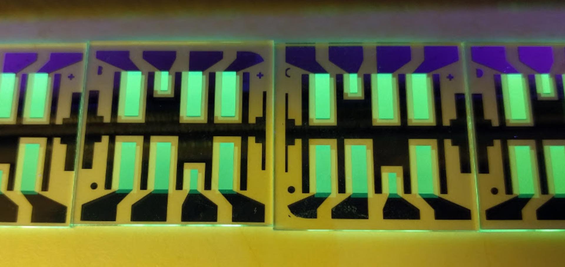
Diindenoperylene derivatives: A model to investigate the path from molecular structure via morphology to solar cell performance
Organic Electronics 14:7 (2013) 1704-1714
Abstract:
Efficient organic electronic devices require a detailed understanding of the relation between molecular structure, thin film growth, and device performance, which is only partially understood at present. Here, we show that small changes in molecular structure of a donor absorber material lead to significant changes in the intermolecular arrangement within organic solar cells. For this purpose, phenyl rings and propyl side chains are fused to the diindenoperylene (DIP) molecule. Grazing incidence X-ray diffraction and variable angle spectroscopic ellipsometry turned out to be a powerful combination to gain detailed information about the thin film growth. Planar and bulk heterojunction solar cells with C60 as acceptor and the DIP derivatives as donor are fabricated to investigate the influence of film morphology on the device performance. Due to its planar structure, DIP is found to be highly crystalline in pristine and DIP:C60 blend films while its derivatives grow liquid-like crystalline. This indicates that the molecular arrangement is strongly disturbed by the steric hindrance induced by the phenyl rings. The high fill factor (FF) of more than 75% in planar heterojunction solar cells of the DIP derivatives indicates excellent charge transport in the pristine liquid-like crystalline absorber layers. However, bulk heterojunctions of these materials surprisingly result in a low FF of only 54% caused by a weak phase separation and thus poor charge carrier percolation paths due to the lower ordered thin film growth. In contrast, crystalline DIP:C60 heterojunctions lead to high FF of up to 65% as the crystalline growth induces better percolation for the charge carriers. However, the major drawback of this crystalline growth mode is the nearly upright standing orientation of the DIP molecules in both pristine and blend films. This arrangement results in low absorption and thus a photocurrent which is significantly lower than in the DIP derivative devices, where the liquid-like crystalline growth leads to a more horizontal molecular alignment. Our results underline the complexity of the molecular structure-device performance relation in organic semiconductor devices. © 2013 Elsevier B.V. All rights reserved.Doping of organic semiconductors
Physica Status Solidi (A) Applications and Materials Science 210:1 (2013) 9-43
Abstract:
The understanding and applications of organic semiconductors have shown remarkable progress in recent years. This material class has been developed from being a lab curiosity to the basis of first successful products as small organic LED (OLED) displays; other areas of application such as OLED lighting and organic photovoltaics are on the verge of broad commercialization. Organic semiconductors are superior to inorganic ones for low-cost and large-area optoelectronics due to their flexibility, easy deposition, and broad variety, making tailor-made materials possible. However, electrical doping of organic semiconductors, i.e. the controlled adjustment of Fermi level that has been extremely important to the success of inorganic semiconductors, is still in its infancy. This review will discuss recent work on both fundamental principles and applications of doping, focused primarily to doping of evaporated organic layers with molecular dopants. Recently, both p- and n-type molecular dopants have been developed that lead to efficient and stable doping of organic thin films. Due to doping, the conductivity of the doped layers increases several orders of magnitude and allows for quasi-Ohmic contacts between organic layers and metal electrodes. Besides reducing voltage losses, doping thus also gives design freedom in terms of transport layer thickness and electrode choice. The use of doping in applications like OLEDs and organic solar cells is highlighted in this review. Overall, controlled molecular doping can be considered as key enabling technology for many different organic device types that can lead to significant improvements in efficiencies and lifetimes. Molecular doping of organic semiconductors has become the key enabling technology for highly efficient and long-living organic light emitting diodes (OLEDs) and made them commercially viable. Other areas of application such as OLED lighting and organic photovoltaics are on the verge of broad commercialization. Again, molecular doping offers many advantages here. However, electrical doping of organic semiconductors, i.e. the controlled adjustment of Fermi level that has been extremely important to the success of inorganic semiconductors, is still in its infancy. This review discusses recent work on both fundamental principles and applications of doping, focused primarily to doping of evaporated organic layers with molecular dopants. Copyright © 2013 WILEY-VCH Verlag GmbH & Co. KGaA, Weinheim.Front Cover: Doping of organic semiconductors (Phys. Status Solidi A 1/2013)
physica status solidi (a) – applications and materials science Wiley 210:1 (2013)
Open-Circuit Voltage and Effective Gap of Organic Solar Cells
Advanced Functional Materials 10:6 (2013)
Abstract:
The open-circuit voltage (V) of an organic solar cell is limited by the donor-acceptor material system. The effective gap E between the electron affinity of the acceptor and the ionization potential of the donor is usually regarded as the upper limit for V, which is only reached for T → 0 K. This relation is confirmed for a number of small-molecule bulk heterojunction p-i-n type solar cells by varying the temperature and illumination intensity. With high precision, the low temperature limit of V is identical to E . Furthermore, the influence of the hole transport material in a p-doped hole transport layer and the donor-acceptor mixing ratio on this limit V is found to be negligible. Varying the active material system, the quantitative relation between V and E is found to be identity. A comparison of V in a series of nine different donor-acceptor material combinations opens a pathway to quantitatively determine the ionization potential of a donor material or the electron affinity of an acceptor material. © 2013 WILEY-VCH Verlag GmbH & Co.Self-passivation of molecular n-type doping during air exposure using a highly efficient air-instable dopant
Physica Status Solidi (A) Applications and Materials Science (2013)


