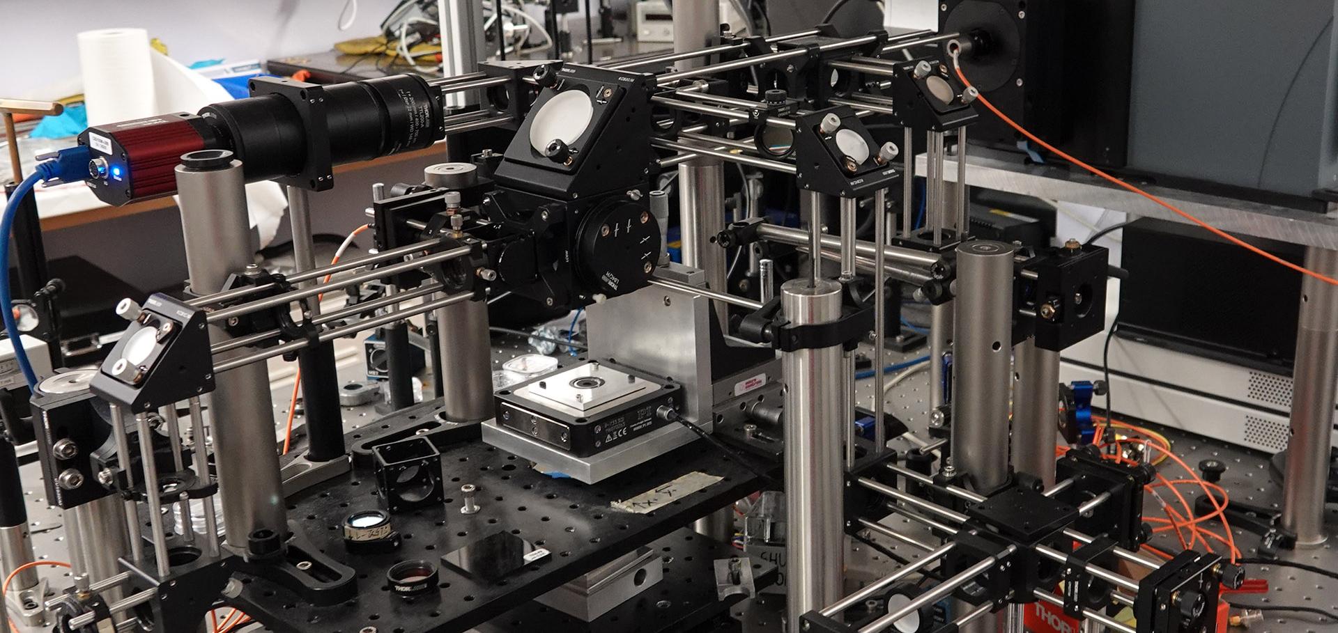
Angled-cage etching of semiconductors (ACES)
The project is part of a joint programme with Prof. Anthony Bennett in Cardiff and Prof. Rachel Oliver in Cambridge funded by the III-V manufacturing hub in Cardiff. It involves developing a novel processing technique to create Gallium Nitride (GaN) optical devices. We are optimising the processing of GaN on various crystal planes by inductively coupled plasma (ICP) using an angled Faraday cage over the sample to create an angled etch. We are examining new geometries for optical cavities which use fewer fabrication steps, simplifying the processing of manufacturable devices.
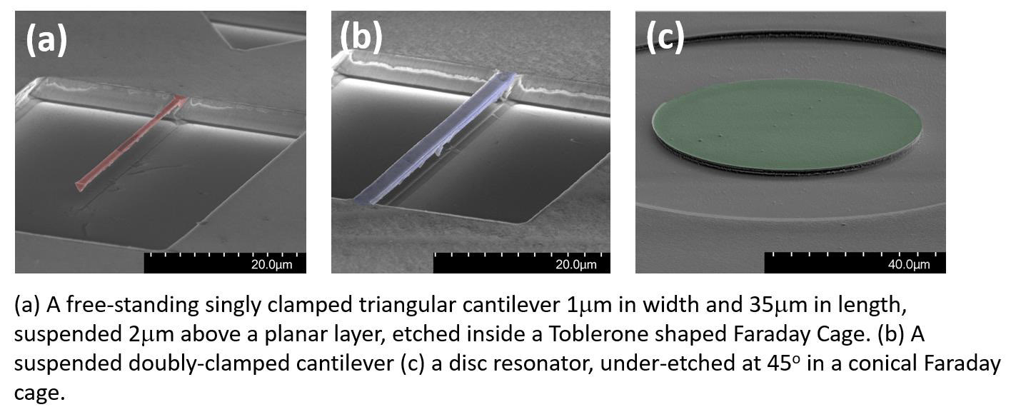
We have already created some photonic crystal beams (which can lead to lasers with ultra-low threshold) and micro-discs (which can be used for lasers, frequency conversion and gas sensing).
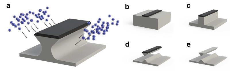
The innovation in the project is the use of a Faraday cage within the ICP tool. The figure below shows how the use of a “triangular prism” Faraday cage would deflect the plasma to create steep angled etches. This technique has not been used in GaN devices before, but offers a particularly elegant and simple method to create optical cavities in GaN. This angled etching eliminates the undercutting step common in silicon-on-insulator and other compound semiconductors, which is crucial as III-Nitrides cannot be undercut. The resulting optical devices will have novel geometries where light is confined by the high reflective index difference between the semiconductor and air.
The project aligns with the Hub activities by focusing on the processing of a commercially important semiconductor, as evidenced by the large number of Hub partners working with III-Nitrides.
A recent publication on this can be found here in AIP Advances from 2020.