Perovskite nanostructures
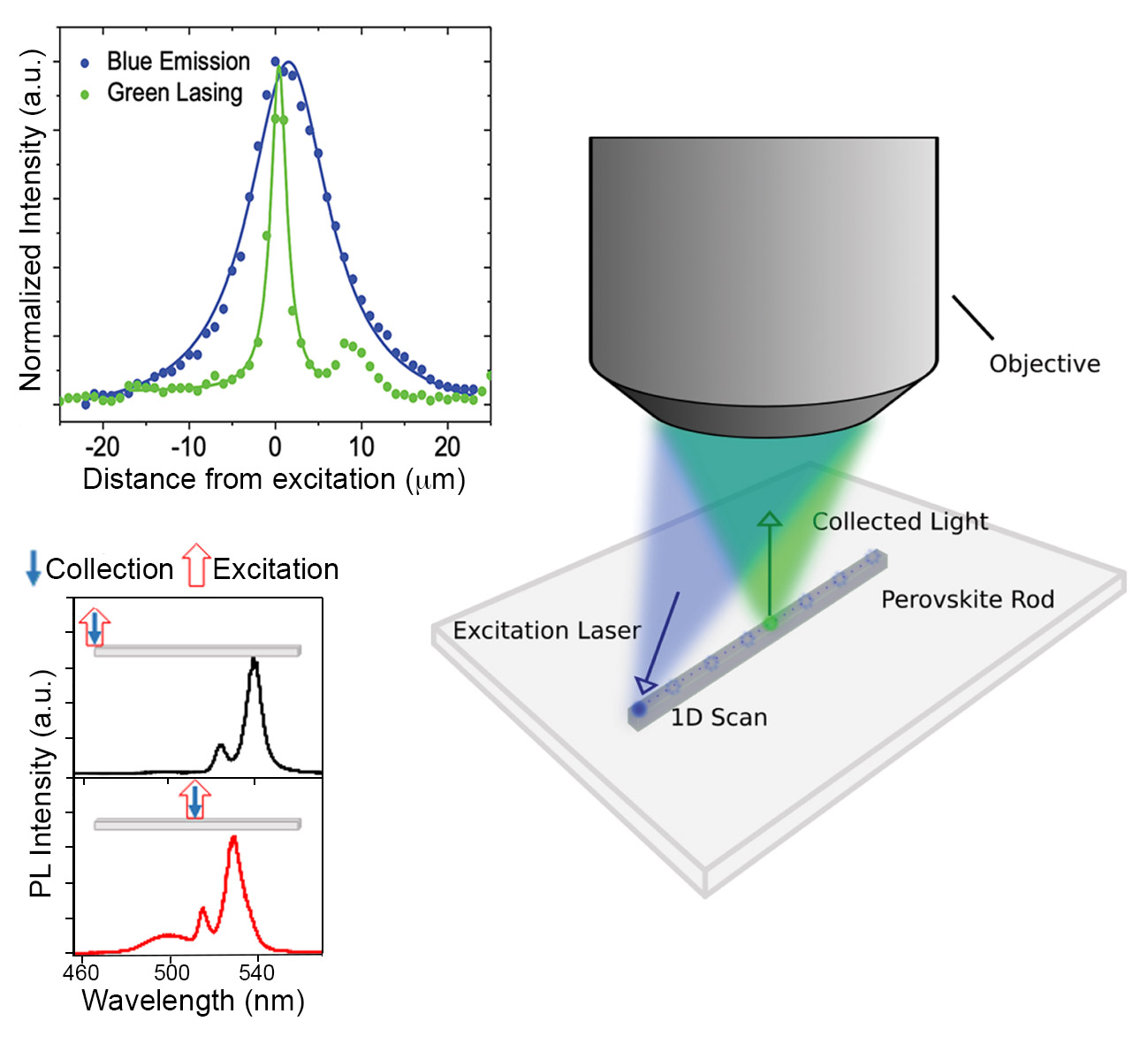
We have been working on emission from nanowires and quantum dots made of perovskites for the past three years. One interesting experiment that we undertook relates to the image above and deals with the effect of surface passivation on the photoluminescence (PL) emitted by CsPbBr3 micro/nano‐rods coated with Pb(OH)2. Here a high quantum yield and excellent stability for the emission were found. The CsPbBr3/Pb(OH)2 rods generally presented a peak that was blue shifted compared to that seen in rods without a hydroxide cladding at low temperatures. By increasing the temperature, we showed that the passivated surface states were very robust against thermal effects and that the PL peak intensity only dropped by a factor of 1.5. Localized stimulated emission at defect states found within larger rods were also demonstrated, clarified by spatially resolved confocal PL mapping along the length of the rods. The diffusion parameter of the carrier density distribution was measured to be 5.70 µm for the sky‐blue emission, whereas for the defect lasing site it was found to be smaller than the excitation spot size. The work was published recently in Advanced Optical Materials.
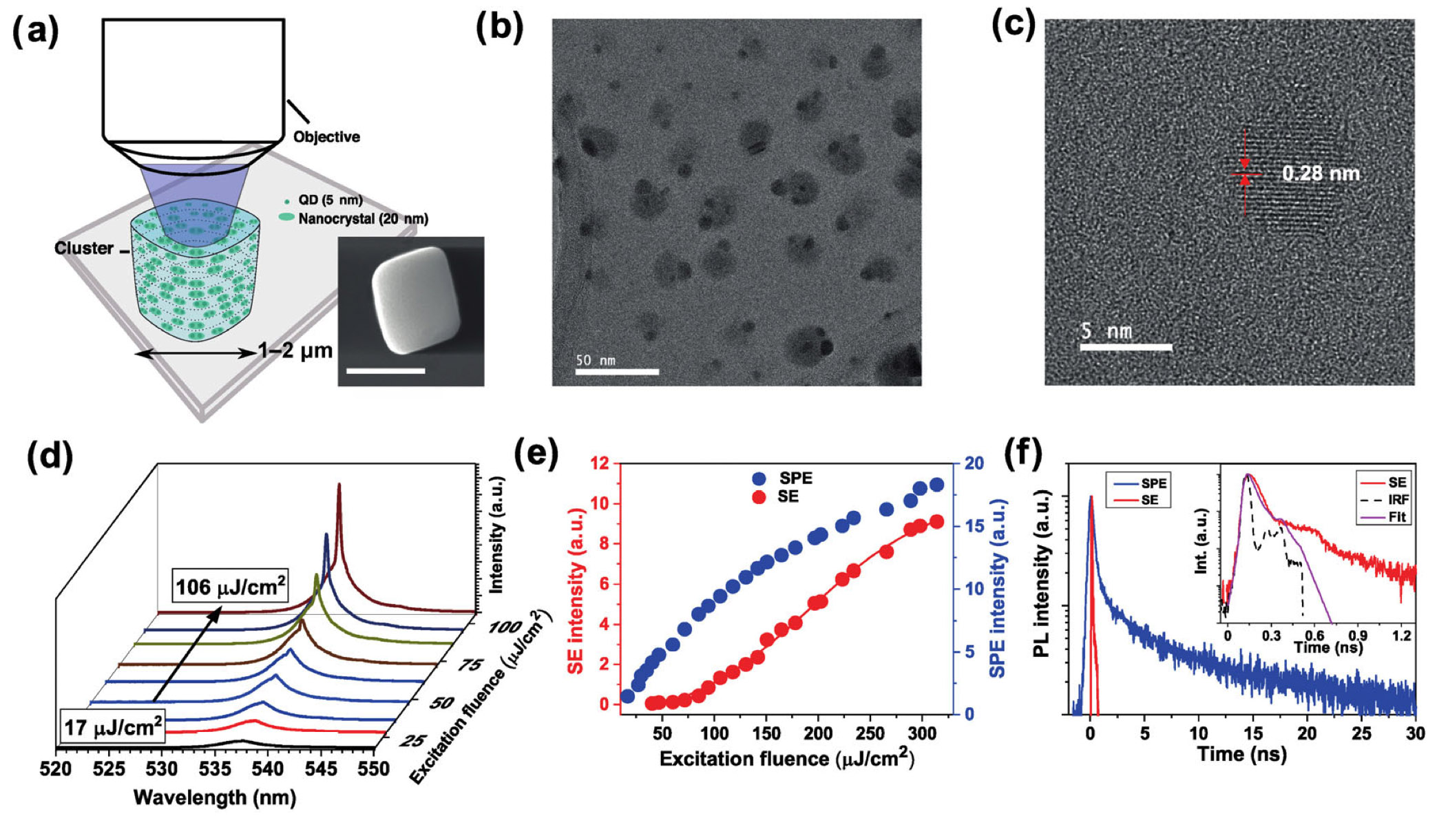
The above image is taken form another recent paper where we looked at the coarse and fine-tuning of lasing transverse electromagnetic modes in coupled all-inorganic perovskite quantum dots. This was was published in Nano Research in 2021. The figure shows (a) a schematic of a self-assembled cluster of nanocrystals. Each nanocrystal comprises two to three CsPbBr3 QDs. The side of the cluster ranges between ~ 1–2 μm, compared to the much smaller nanocrystals ~ 20 nm in diameter. The laser excitation area illuminates hundreds of nanocrystals. Bottom right is an SEM image of a cluster (scale bar is 1 μm). (b) Transmission electron microscope image of CsPbBr3 QDs inside a cluster. The dark spots inside the clusters are individual QDs (diameter of ~ 5 nm). (c) High-resolution transition electron microscope image of a QD, highlighting the crystallinity of the assembly with a lattice spacing of 0.28 nm. (d) Power-dependent PL spectra at a low excitation fluence regime below ~ 106 μJ/cm2. Each spectrum shows a broad background SPE with a FWHM of ~ 3 nm due to the ensemble effect. (e) Integrated emission intensity of the background SPE and the sharp lasing peak (with the SPE subtracted) as a function of excitation power. An S-shape characteristic of lasing can be seen for the SE trace, with an onset and saturation, while the intensity of the SPE emission continues to increase linearly. (f) Time resolved photoluminescence at ~ 200 μJ/cm2 for the SE and SPE signals at a low excitation fluence ~ 95 nJ/cm2, with the inset detailing the same decay within the first nanosecond.