Photonic crystal cavities
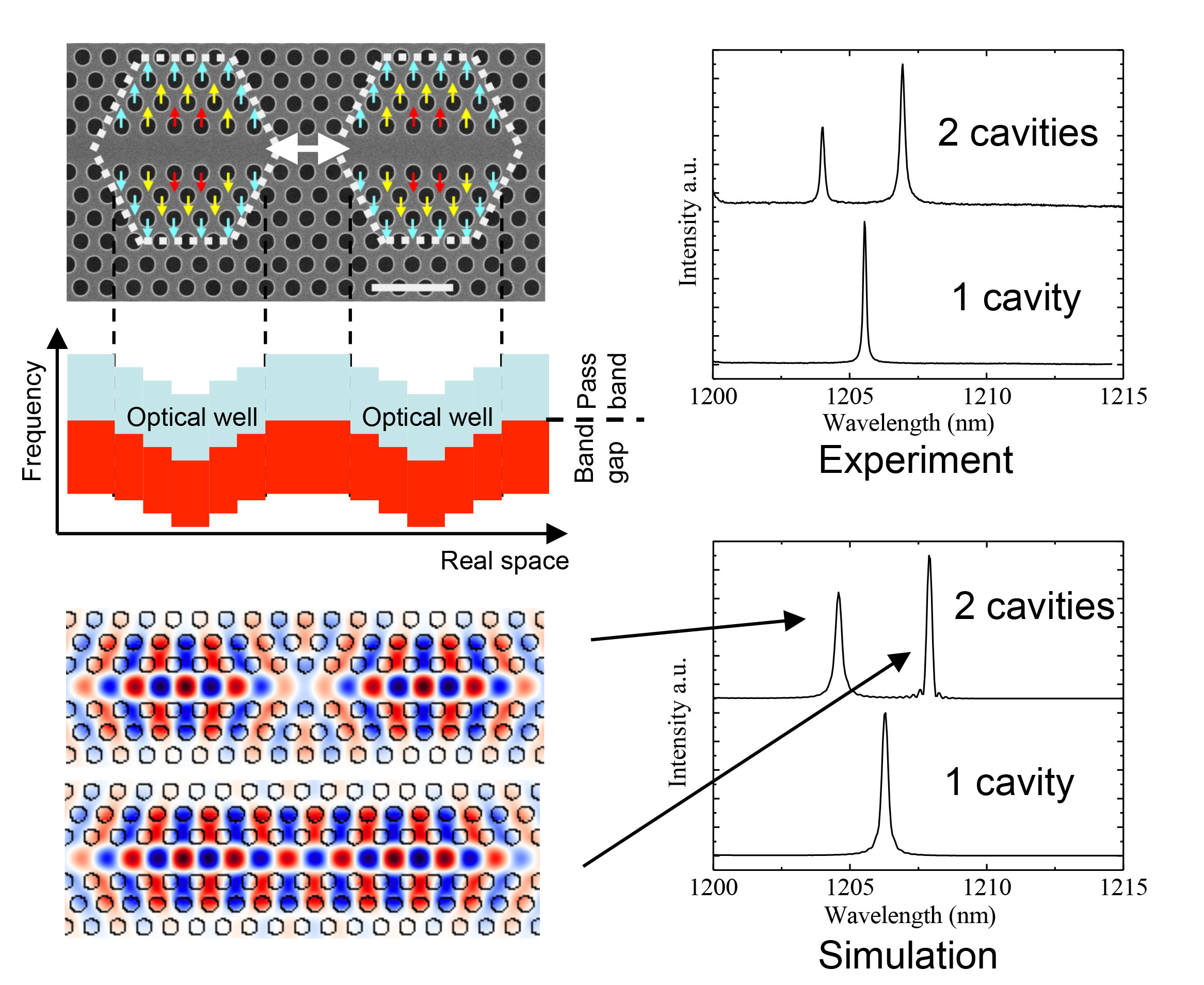
The figure above shows a scanning eletron microscope image of a coupled photonic crystal waveguide cavity with embedded InGaAs quantum dots. The shifted holes produce a reduction in the local potential producing two coupled optical wells as shown in the schematic energy diagram below the imnage. At the bottom a finite difference time domain calculation of the expected electric field pattern is seen, together with a simulation of the luminescence intensity expected from a single cavity and from the coupled cavity. The graph on the top right shows the experimentally measured emission from the cavity structure in the SEM image, showing excellent agreement to the simulation.
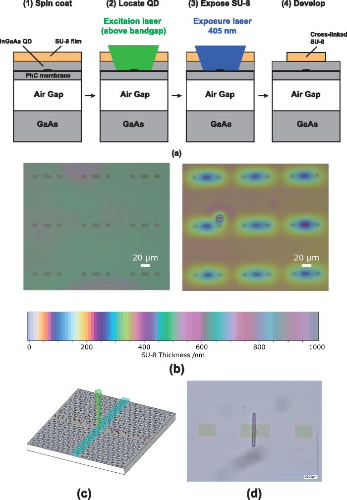
Recently we published work in Applied Physics Letters on Purcell enhancement of a deterministically coupled quantum dot in an SU-8 laser patterned photonic crystal heterostructure. The figure above shows (a) cavity fabrication via laser exposure of SU-8 at 4 K. (b) A microscope image of the spin-coated SU-8 thin film with the colour scale for thickness reference; left: coated uniform film of ∼500 nm thickness; right: Thinning of the SU-8 film on top of the photonic crystal for a thin spin-coated layer (about 300 nm thick). (c) 3D schematic of the SU-8 strip cavity. The green transparent cone represents excitation laser 532 nm. The cyan strip marks the cavity, and red dots represent quantum dots. (d) An image of our fabricated cavity.
The emission is enhanced by the cavity producing a maximum Purcell factor of
\(F_p = \frac{3}{4\pi^2}\left(\frac{\lambda}{n}\right)^3 \left(\frac{Q}{V}\right)\)
which, for the Q factor of 2000 for our cavity produces a maximum theoretical value of 117. Imperfections in the crystal and the alignment of the quantum dot with the cavity mean that the actual measured enhancement was 2.16.