World-class vacuum deposition capabilities to develop next-gen advanced functional materials
This national facility provides state-of-the-art vacuum deposition equipment to enable the development of next generation advanced functional materials. The bespoke cluster tool comprises several interconnected vacuum chambers – rather than existing isolated deposition chambers – allowing for the creation of multilayer structures using a range of different processes and combining materials that cannot done in the same vacuum chamber. The National Thin-Film Cluster Facility for Advanced Functional Materials (NTCF) is key to the UK’s R&D capabilities in the development of next-generation materials and devices for application in energy, photonics and electronics.
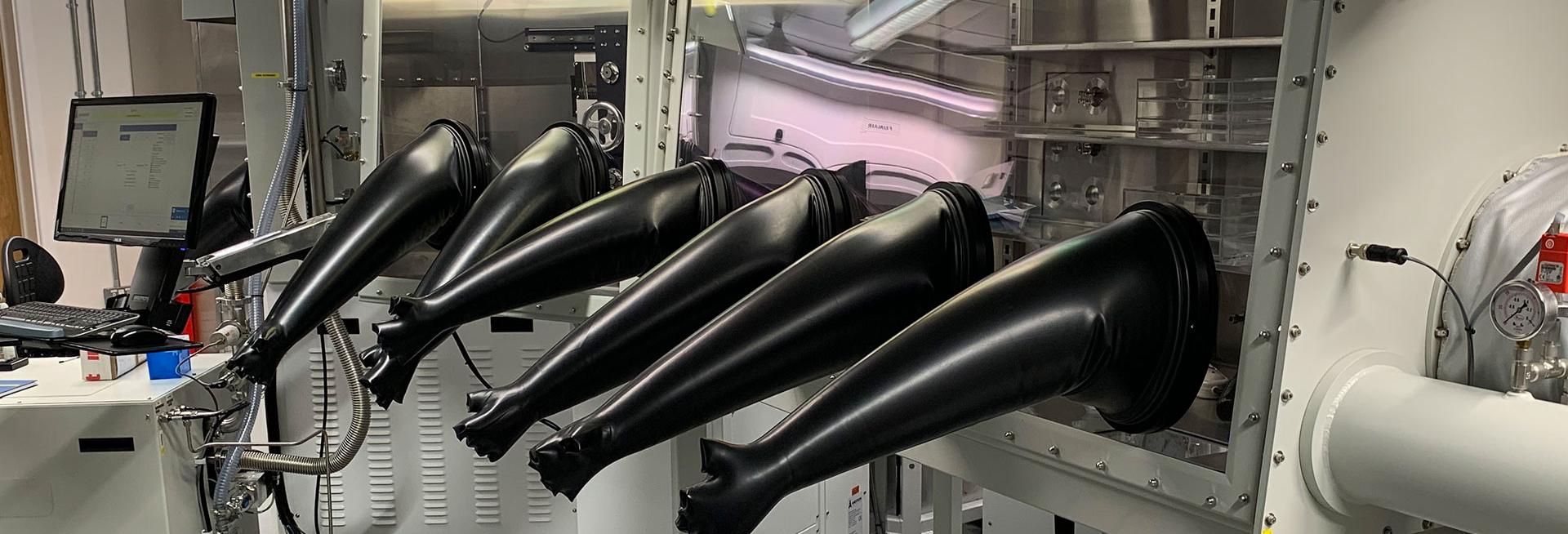
Five deposition chambers
The facility allows for unprecedented process control and versatility and has been designed such that all chambers can be used in parallel by several users simultaneously, maximising the potential research output. The NTCF’s initial five thin-film deposition chambers – two organic thermal deposition chambers, one perovskite thermal deposition chamber, one sputter chamber, and a chamber for atomic layer deposition – are connected by handler units that enable transfer under vacuum conditions and the various deposition processes enable close control of the thickness (<1 to >100 nanometres) and composition of each layer of the material.
Controlled vacuum environment
The facility, co-directed by Professor Henry Snaith and Professor Moritz Riede, is housed in a dedicated laboratory refurbished specifically for this purpose in the Department of Physics. A national collaboration with co-investigators from the Universities of Cambridge and Loughborough and Imperial College London, the facility has been funded by the UK’s EPSRC, the Wolfson Foundation and the University of Oxford.
Research priorities
The NTCF initially focusses on three material groups: perovskites for use in optoelectronics with applications ranging across solar energy, displays and electronic circuits; exploring the potential of organic semiconductors – already used in the latest generation of displays for television screens and mobile phones – and extending this success to other applications like organic solar energy; and research into metal oxides, the transparent electrode used in a variety of devices and with the potential to be used as transistors to drive a new generation of displays.
Contact
Jin Yao, Facility Manager