Home
Department Of Physics text logo
  • Research
    • Our research
    • Our research groups
    • Our research in action
    • Research funding support
    • Summer internships for undergraduates
  • Study
    • Undergraduates
    • Postgraduates
  • Engage
    • For alumni
    • For business
    • For schools
    • For the public
Menu
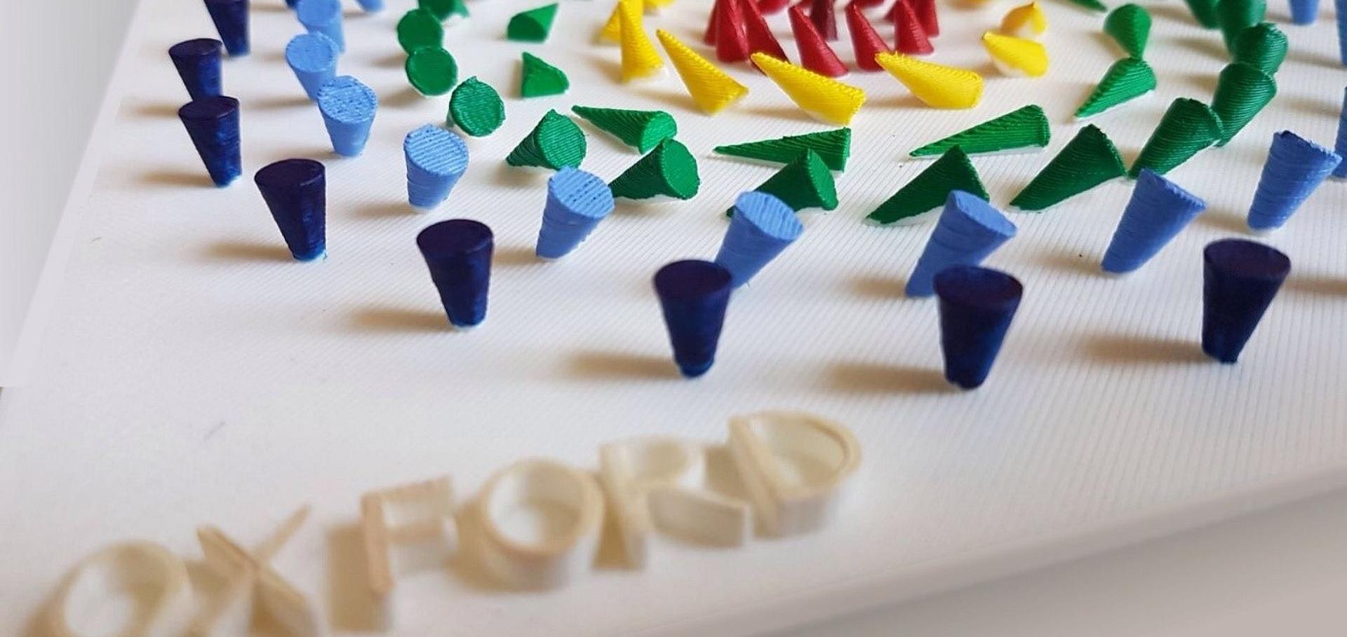
Magnetic skyrmions

Professor Thorsten Hesjedal FInstP

Professor of Condensed Matter Physics

Research theme

  • Quantum materials

Sub department

  • Condensed Matter Physics

Research groups

  • Thin film quantum materials
  • Oxford Quantum Institute
  • Magnetism for Intelligent Devices (MIND)
Thorsten.Hesjedal@physics.ox.ac.uk
Telephone: 01865 (2)72235
  • About
  • Publications

Field dependence of micromagnetic domain patterns in MnAs films

Journal of Applied Physics 98:6 (2005)

Authors:

R Engel-Herbert, T Hesjedal, J Mohanty, DM Schaadt, KH Ploog

Abstract:

We have studied the domain behavior of submicrometer wide ferromagnetic stripes by magnetic force microscopy (MFM) in the presence of an in situ magnetic field. MFM images in the demagnetized state show alternatingly magnetized domains fully extended across the stripe. Moreover, domain structures are found to exhibit a substructure across the stripe. Increasing fields drive out the domain walls of the complex domains first, leaving the alternating domains behind. The remaining magnetization process aligns increasing parts of the domains along the field direction by gradually shrinking the width of oppositely magnetized domains rather than by flipping larger areas at once. Micromagnetic simulations confirm the observed behavior. The simulations reveal that flipping of the domains occurs only when a magnetic pinning center is involved. © 2005 American Institute of Physics.
More details from the publisher
More details

A microscopic view on acoustomigration.

IEEE Trans Ultrason Ferroelectr Freq Control 52:9 (2005) 1584-1593

Authors:

Thorsten Hesjedal, Jyoti Mohanty, Franz Kubat, Werner Ruile, Leonhard M Reindl

Abstract:

Stress-induced material transport in surface acoustic wave devices, so-called acoustomigration, is a prominent failure mechanism, especially in high-power applications. We used scanning probe microscopy techniques to study acoustomigration of metal structures in-situ, i.e., during the high-power loading of the device. Scanning acoustic force microscopy (SAFM) allows for the simultaneous measurement of the acoustic wavefield and the topography with submicron lateral resolution. High-resolution microscopy is essential as acoustomigration is a phenomenon that not only results in the formation of more macroscopic voids and hillocks but also affects the microscopic grain structure of the film. We present acoustic wavefield and topographic image sequences giving a clear insight into the nature of the film damage on a submicron scale. The 900 MHz test structures were fabricated on 36 degrees YX-lithium tantalate (YX-LiTaO3) and incorporated 420-nm thick aluminium (Al) electrodes. By correlating the acoustic wavefield mapping and the local changes in topography, we confirmed model calculations that predict the correspondence of damage and stress (i.e., hillocks and voids) are preferentially formed in areas of high stress. The way the film is damaged does not significantly depend on the applied power (for typical power levels used in this study). Furthermore, acoustomigration leads to smoother surfaces via lateral grain growth. Another contribution to the grain dynamics comes from the apparent grain rotation in the highly anisotropic stress field of an acoustic wave. Thus, through in-situ scanning probe microscopy techniques, one can observe the initial changes of the grain structure in order to obtain a more detailed picture of the phenomenon of acoustomigration.
More details from the publisher
More details

Selective etching of epitaxial MnAs films on GaAs(001): Influence of structure and strain

Journal of Applied Physics 98:1 (2005)

Authors:

J Mohanty, Y Takagaki, T Hesjedal, L Däweritz, KH Ploog

Abstract:

Strain in epitaxial MnAs thin films on GaAs(001) substrates plays an important role in the coupled magnetostructural phase transition. As a result of strain, the phase transition from the ferromagnetic α phase to the paramagnetic Β phase proceeds over a wide temperature range and the coexisting phases form a periodic stripe array. Employing suitable wet chemical etchants, the two MnAs phases can be etched selectively. Perpendicular to the α-Β -stripe structure, the built-up strain relaxes in the course of the etching process by the formation of cracks. The combination of both strain relaxation mechanisms allows for the defined patterning of two-dimensional arrays of nanomagnets. Through micromagnetic investigations, it is possible to identify the location of α - and Β-MnAs which helps to clarify two major aspects of the etching process. First, it is possible to determine the etch rates of α - and Β-MnAs and follow the complex interplay of strain and phase composition during the etching process. Second, as strain reflects itself in a shifted phase-transition temperature, temperature-dependent micromagnetic studies allow to determine the strain environment of the cracks. © 2005 American Institute of Physics.
More details from the publisher
More details

Nanofabrication for Surface-Acoustic-Wave Devices

Chapter in Nanotechnology focus, Nova Science Pub Inc (2005) 1

Authors:

T Hesjedal, W Seidel

Abstract:

This book presents the latest research in this frontier field.

Calculation of the magnetic stray field of a uniaxial magnetic domain

Journal of Applied Physics 97:7 (2005)

Authors:

R Engel-Herbert, T Hesjedal

Abstract:

We present an analytic solution for the magnetic field of a bar-shaped permanent magnet. Assuming a constant magnetization, we derive expressions for the stray field in three dimensions. The analytic solutions can be readily applied to field calculation problems for magnetic force microscopy simulations without the need for finite element methods. © 2005 American Institute of Physics.
More details from the publisher
More details

Pagination

  • First page First
  • Previous page Prev
  • …
  • Page 54
  • Page 55
  • Page 56
  • Page 57
  • Current page 58
  • Page 59
  • Page 60
  • Page 61
  • Page 62
  • …
  • Next page Next
  • Last page Last

Footer Menu

  • Contact us
  • Giving to the Dept of Physics
  • Work with us
  • Media

User account menu

  • Log in

Follow us

FIND US

Clarendon Laboratory,

Parks Road,

Oxford,

OX1 3PU

CONTACT US

Tel: +44(0)1865272200

University of Oxfrod logo Department Of Physics text logo
IOP Juno Champion logo Athena Swan Silver Award logo

© University of Oxford - Department of Physics

Cookies | Privacy policy | Accessibility statement

Built by: Versantus

  • Home
  • Research
  • Study
  • Engage
  • Our people
  • News & Comment
  • Events
  • Our facilities & services
  • About us
  • Current students
  • Staff intranet