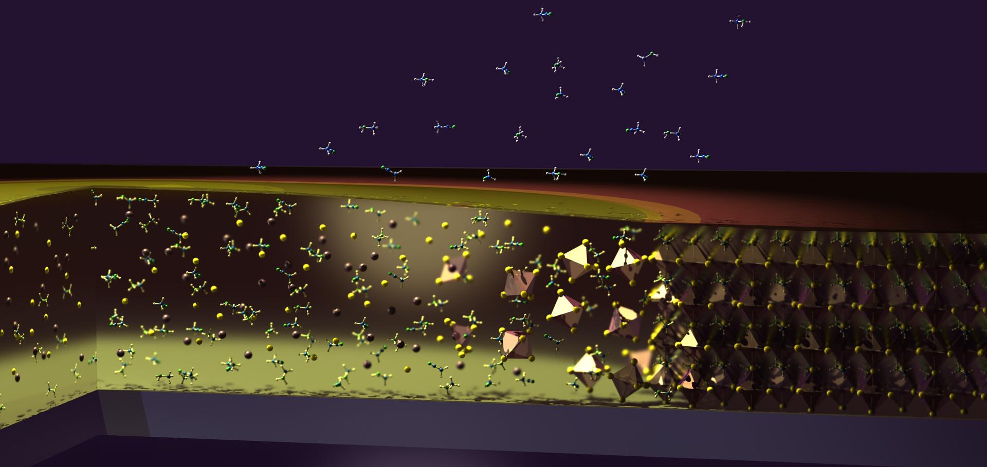

My research lies at the intersection of solid-state physics, chemistry, and materials science, with the aim of uncovering the fundamental processes that govern thin-film crystallisation and defect formation in semiconductor materials. Currently, I focus on elucidating the intricate relationships between precursor chemistry, crystallisation kinetics, and defect formation in metal halide perovskites fabricated using both solution-based and vapour-phase deposition approaches. By combining advanced nanoscale characterisation techniques with measurements of bulk thin-film properties, my work seeks to disentangle how atomic level interactions and phase evolution pathways influence thin-film morphology, defect landscapes, and the optoelectronic properties of thin-films and devices.
These insights are intended to bridge the gap between fundamental chemical mechanisms and practical materials and device physics; enabling the rational design of new precursor systems, solvent environments, and deposition modalities tailored towards high-performance semiconductor thin films. Ultimately, the overarching goal of my research is to translate this fundamental understanding into tangible performance improvements in perovskite-based optoelectronic devices, particularly high-efficiency solar cells and light-emitting diodes (LEDs), while providing guiding principles for the development of the next generation of semiconductors.