Home
Department Of Physics text logo
  • Research
    • Our research
    • Our research groups
    • Our research in action
    • Research funding support
    • Summer internships for undergraduates
  • Study
    • Undergraduates
    • Postgraduates
  • Engage
    • For alumni
    • For business
    • For schools
    • For the public
Menu
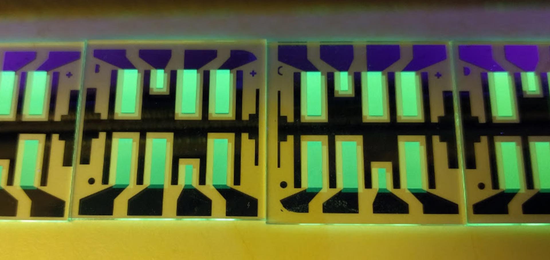
One of the substrate layouts for our organic solar cells
Credit: AFMD Group

Moritz Riede

Professor of Soft Functional Nanomaterials

Research theme

  • Photovoltaics and nanoscience

Sub department

  • Condensed Matter Physics

Research groups

  • Advanced Functional Materials and Devices (AFMD) Group
moritz.riede@physics.ox.ac.uk
Telephone: 01865 (2)72377 (office),01865 (2)82095 (lab)
  • About
  • Research
  • Teaching
  • Publications

Doping Carbon Nanotube Ethylene-Vinyl Acetate Thin Films for Touch-Sensitive Applications

ACS Applied Electronic Materials American Chemical Society 7:11 (2025) 4738-4746

Authors:

Bernd K Sturdza, Nicole Jacobus, Andre Bennett, Joshua Form, Louis Wood, M Greyson Christoforo, Moritz K Riede, Robin J Nicholas

Abstract:

Transparent conductive films are key components of many optoelectronic devices but are often made from either scarce or brittle materials like indium tin oxide. Carbon nanotube-polymer films offer an abundant and flexible alternative. Here, we report how the dimensions of the carbon nanotube raw material affect their thin film performance and thickness yield when processed with the polymer ethylene-vinyl acetate. We perform chemical doping with several halogenated metals and find the electron affinity of the metal to be a good indicator of p-doping effectiveness. We identify CuCl2 as low-cost alternative to the established gold chloride dopants. Optimising the dopant deposition method allows us to reduce the effect of doping on the optical transmittance. Percolation analysis of our films demonstrates that optimized single-walled carbon nanotube-ethylene-vinyl acetate films show no sign of percolation effects down to thicknesses of 5 nm. Finally, we produce transparent touch-sensitive devices. Comparing several of these devices, we find a linear relationship between the sheet resistance and the on/off ratio of the touch sensing that can be used to determine a threshold film thickness. Using doped carbon nanotube-ethylene-vinyl acetate films increases the on/off ratio and allows us to fabricate touch-sensitive devices with an on/off ratio of 10 at 95% optical transmittance. This clearly demonstrates the potential of these films for transparent touch-sensitive applications.
More details from the publisher
Details from ORA
More details
More details

Direct visualization of the charge transfer state dynamics in dilute-donor organic photovoltaic blends

Nature Communications Springer Nature 15:1 (2024) 9851

Authors:

Gareth John Moore, Florian Günther, Kaila M Yallum, Martina Causa’, Anna Jungbluth, Julien Réhault, Moritz Riede, Frank Ortmann, Natalie Banerji

Abstract:

The interconversion dynamics between charge transfer state charges (CTCs) and separated charges (SCs) is still an unresolved issue in the field of organic photovoltaics. Here, a transient absorption spectroscopy (TAS) study of a thermally evaporated small-molecule:fullerene system (α6T:C60) in different morphologies (dilute intermixed and phase separated) is presented. Spectral decomposition reveals two charge species with distinct absorption characteristics and different dynamics. Using time-dependent density functional theory, these species are identified as CTCs and SCs, where the spectral differences arise from broken symmetry in the charge transfer state that turns forbidden transitions into allowed ones. Based on this assignment, a kinetic model is formulated allowing the characterization of the charge generation, separation, and recombination mechanisms. We find that SCs are either formed directly from excitons within a few picoseconds or more slowly (~30–80 ps) from reversible splitting of CTCs. These findings constitute the first unambiguous observation of spectrally resolved CTCs and SCs.
More details from the publisher
Details from ORA
More details
More details

From generation to collection – impact of deposition temperature on charge carrier dynamics of high-performance vacuum-processed organic solar cells

Energy & Environmental Science Royal Society of Chemistry (RSC) (2024)

Authors:

Richard Adam Pacalaj, Yifan Dong, Ivan Ramirez, Roderick CI MacKenzie, Seyed Mehrdad Hosseini, Eva Bittrich, Julian Eliah Heger, Pascal Kaienburg, Subhrangsu Mukherjee, Jiaying Wu, Moritz Riede, Harald Ade, Peter Müller-Buschbaum, Martin Pfeiffer, James Robert Durrant

Abstract:

<jats:p>Substrate heating during co-evaporation of bulk heterojunction organic solar cells aids phase separation and improves performance. While recombination remains unaffected, hole transport improves due to more crystalline donor domains.</jats:p>
More details from the publisher
Details from ORA
More details

Roadmap on established and emerging photovoltaics for sustainable energy conversion

JPhys Energy IOP Publishing 6:4 (2024) 041501

Authors:

James C Blakesley, Ruy S Bonilla, Marina Freitag, Alex M Ganose, Nicola Gasparini, Pascal Kaienburg, George Koutsourakis, Jonathan D Major, Jenny Nelson, Nakita K Noel, Bart Roose, Jae Sung Yun, Simon Aliwell, Pietro P Altermatt, Tayebeh Ameri, Virgil Andrei, Ardalan Armin, Diego Bagnis, Jenny Baker, Hamish Beath, Mathieu Bellanger, Philippe Berrouard, Jochen Blumberger, Stuart A Boden, Marina R Filip, Elizabeth A Gibson, M Saiful Islam, Michael B Johnston

Abstract:

Photovoltaics (PVs) are a critical technology for curbing growing levels of anthropogenic greenhouse gas emissions, and meeting increases in future demand for low-carbon electricity. In order to fulfill ambitions for net-zero carbon dioxide equivalent (CO2eq) emissions worldwide, the global cumulative capacity of solar PVs must increase by an order of magnitude from 0.9 TWp in 2021 to 8.5 TWp by 2050 according to the International Renewable Energy Agency, which is considered to be a highly conservative estimate. In 2020, the Henry Royce Institute brought together the UK PV community to discuss the critical technological and infrastructure challenges that need to be overcome to address the vast challenges in accelerating PV deployment. Herein, we examine the key developments in the global community, especially the progress made in the field since this earlier roadmap, bringing together experts primarily from the UK across the breadth of the PVs community. The focus is both on the challenges in improving the efficiency, stability and levelized cost of electricity of current technologies for utility-scale PVs, as well as the fundamental questions in novel technologies that can have a significant impact on emerging markets, such as indoor PVs, space PVs, and agrivoltaics. We discuss challenges in advanced metrology and computational tools, as well as the growing synergies between PVs and solar fuels, and offer a perspective on the environmental sustainability of the PV industry. Through this roadmap, we emphasize promising pathways forward in both the short- and long-term, and for communities working on technologies across a range of maturity levels to learn from each other.
More details from the publisher
Details from ORA
More details

Strategies to Control Crystal Growth of Highly Ordered Rubrene Thin Films for Application in Organic Photodetectors

Advanced Optical Materials Wiley (2024)

Authors:

Anna‐Lena Hofmann, Jakob Wolansky, Mike Hambsch, Felix Talnack, Eva Bittrich, Lucy Winkler, Max Herzog, Tianyi Zhang, Tobias Antrack, L Conrad Winkler, Jonas Schröder, Moritz Riede, Stefan CB Mannsfeld, Johannes Benduhn, Karl Leo

Abstract:

<jats:title>Abstract</jats:title><jats:p>Organic semiconductors still lag behind their inorganic counterparts in terms of mobility due to their lower structural order, in particular in thin films. Here, the highly ordered phase of triclinic rubrene – characterized by high vertical hole mobility – grown from a vacuum‐deposited thin film is used by post‐annealing and implemented into organic photodetectors. Since the triclinic rubrene exhibits a high roughness with a peak‐to‐valley value of 250 nm, which is detrimental to the dark current, strategies to control the crystal growth are developed. These investigations show that a suppression layer of 20 nm C<jats:sub>60</jats:sub> is the most promising approach to successfully reduce the surface roughness while maintaining the triclinic phase, proven by grazing‐incidence wide‐angle X‐ray scattering (GIWAXS). With the smoothened active layer, the dark current density is reduced by three orders of magnitude compared to the neat rubrene layer. It is as low as 2.5 × 10<jats:sup>−10 </jats:sup>A cm<jats:sup>−2</jats:sup> at −0.1 V bias, reflected in an overall specific detectivity of 6 × 10<jats:sup>11</jats:sup> Jones at zero bias (based on noise measurements) and a high linear dynamic range of 170 dB. This strategy using a suppression layer thus proves successful and is very promising to be applied to other crystalline materials.</jats:p>
More details from the publisher
Details from ORA
More details

Pagination

  • First page First
  • Previous page Prev
  • Page 1
  • Current page 2
  • Page 3
  • Page 4
  • Page 5
  • Page 6
  • Page 7
  • Page 8
  • Page 9
  • …
  • Next page Next
  • Last page Last

Footer Menu

  • Contact us
  • Giving to the Dept of Physics
  • Work with us
  • Media

User account menu

  • Log in

Follow us

FIND US

Clarendon Laboratory,

Parks Road,

Oxford,

OX1 3PU

CONTACT US

Tel: +44(0)1865272200

University of Oxfrod logo Department Of Physics text logo
IOP Juno Champion logo Athena Swan Silver Award logo

© University of Oxford - Department of Physics

Cookies | Privacy policy | Accessibility statement

Built by: Versantus

  • Home
  • Research
  • Study
  • Engage
  • Our people
  • News & Comment
  • Events
  • Our facilities & services
  • About us
  • Giving to Physics
  • Current students
  • Staff intranet