

Cavity-enhanced blue single-photon emission from a single InGaN/GaN quantum dot
APPLIED PHYSICS LETTERS 91:5 (2007) ARTN 052101
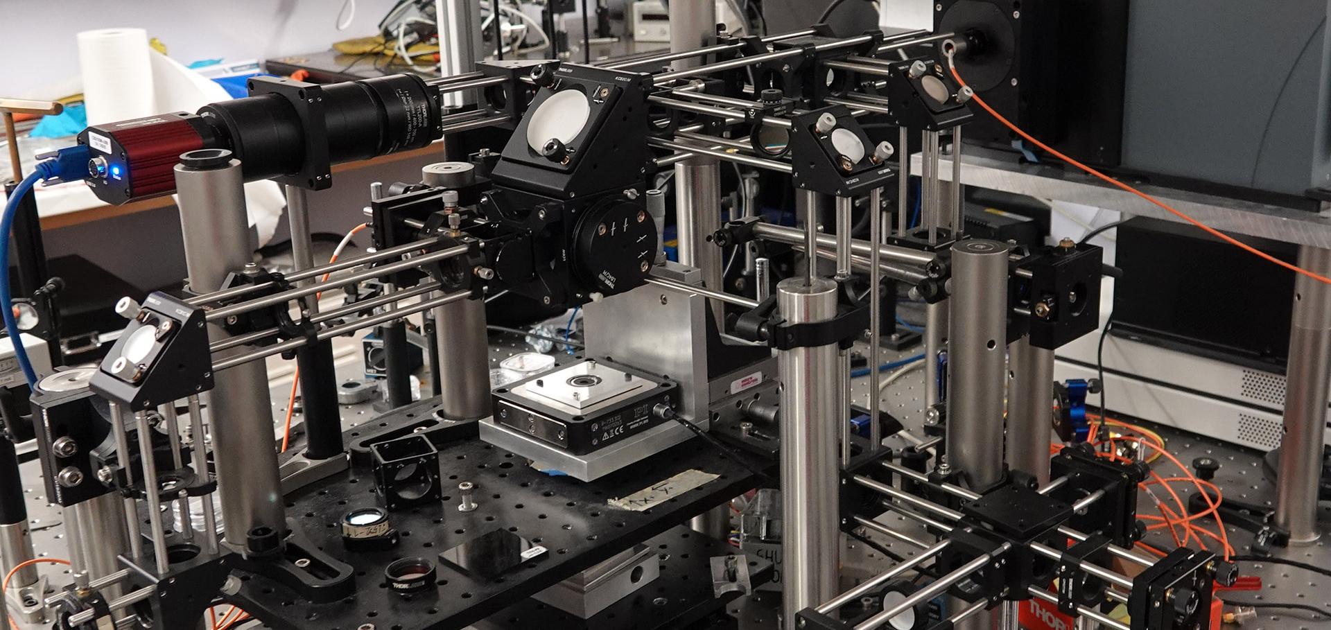
Characterization of Tunneling and Free-Carrier Screening in Coupled Asymmetric GaN/AlGaN Quantum Discs
AIP Conference Proceedings AIP 893 (2007) 1003-1004
Characterization of tunneling and free-carrier screening in coupled asymmetric GaN/AlGaN quantum discs
AIP CONF PROC 893 (2007) 1003-1004
Abstract:
We present a systematic investigation of free-carrier screening in coupled asymmetric GaN quantum discs with embedded AlGaN barriers using time-integrated and time-resolved micro-photoluminescence measurements, supported by three-dimensional multi-band k.p computational modeling. Free-carrier screening effects decreased with the barrier thickness, which indicates that the source of the free-carriers were carriers tunneling through the barrier.Comparison of exciton optical nonlinearities for resonant and non-resonant excitation
JOURNAL OF THE KOREAN PHYSICAL SOCIETY 51:1 (2007) 149-154
Creating diamond color centers for quantum optical applications
DIAMOND AND RELATED MATERIALS 16:11 (2007) 1887-1895