Holographic definition of photonic crystal structures.
ABSTRACTS OF PAPERS OF THE AMERICAN CHEMICAL SOCIETY 221 (2001) U245-U245
Photonic crystals made by holographic lithography
MRS BULLETIN 26:8 (2001) 632-636
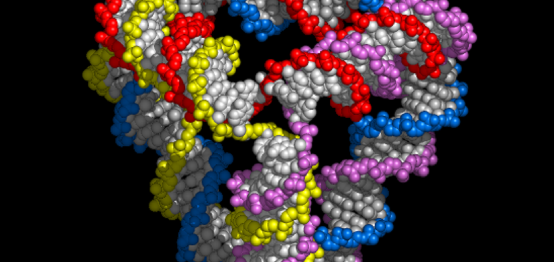
A DNA-fuelled molecular machine made of DNA.
Nature 406:6796 (2000) 605-608
Abstract:
Molecular recognition between complementary strands of DNA allows construction on a nanometre length scale. For example, DNA tags may be used to organize the assembly of colloidal particles, and DNA templates can direct the growth of semiconductor nanocrystals and metal wires. As a structural material in its own right, DNA can be used to make ordered static arrays of tiles, linked rings and polyhedra. The construction of active devices is also possible--for example, a nanomechanical switch, whose conformation is changed by inducing a transition in the chirality of the DNA double helix. Melting of chemically modified DNA has been induced by optical absorption, and conformational changes caused by the binding of oligonucleotides or other small groups have been shown to change the enzymatic activity of ribozymes. Here we report the construction of a DNA machine in which the DNA is used not only as a structural material, but also as 'fuel'. The machine, made from three strands of DNA, has the form of a pair of tweezers. It may be closed and opened by addition of auxiliary strands of 'fuel' DNA; each cycle produces a duplex DNA waste product.Fabrication of photonic crystals for the visible spectrum by holographic lithography.
Nature 404:6773 (2000) 53-56
Abstract:
The term 'photonics' describes a technology whereby data transmission and processing occurs largely or entirely by means of photons. Photonic crystals are microstructured materials in which the dielectric constant is periodically modulated on a length scale comparable to the desired wavelength of operation. Multiple interference between waves scattered from each unit cell of the structure may open a 'photonic bandgap'--a range of frequencies, analogous to the electronic bandgap of a semiconductor, within which no propagating electromagnetic modes exist. Numerous device principles that exploit this property have been identified. Considerable progress has now been made in constructing two-dimensional structures using conventional lithography, but the fabrication of three-dimensional photonic crystal structures for the visible spectrum remains a considerable challenge. Here we describe a technique--three-dimensional holographic lithography--that is well suited to the production of three-dimensional structures with sub-micrometre periodicity. With this technique we have made microperiodic polymeric structures, and we have used these as templates to create complementary structures with higher refractive-index contrast.Low-energy electronic spin excitations between filling factors ν = 1 and 1/2 studied by optically detected nuclear magnetic resonance
Physica E: Low-Dimensional Systems and Nanostructures 6:1 (2000) 56-59