Optoelectronic properties of mixed iodide-bromide perovskites from first-principles computational modeling and experiment
Journal of Physical Chemistry Letters American Chemical Society 13:18 (2022) 4184-4192
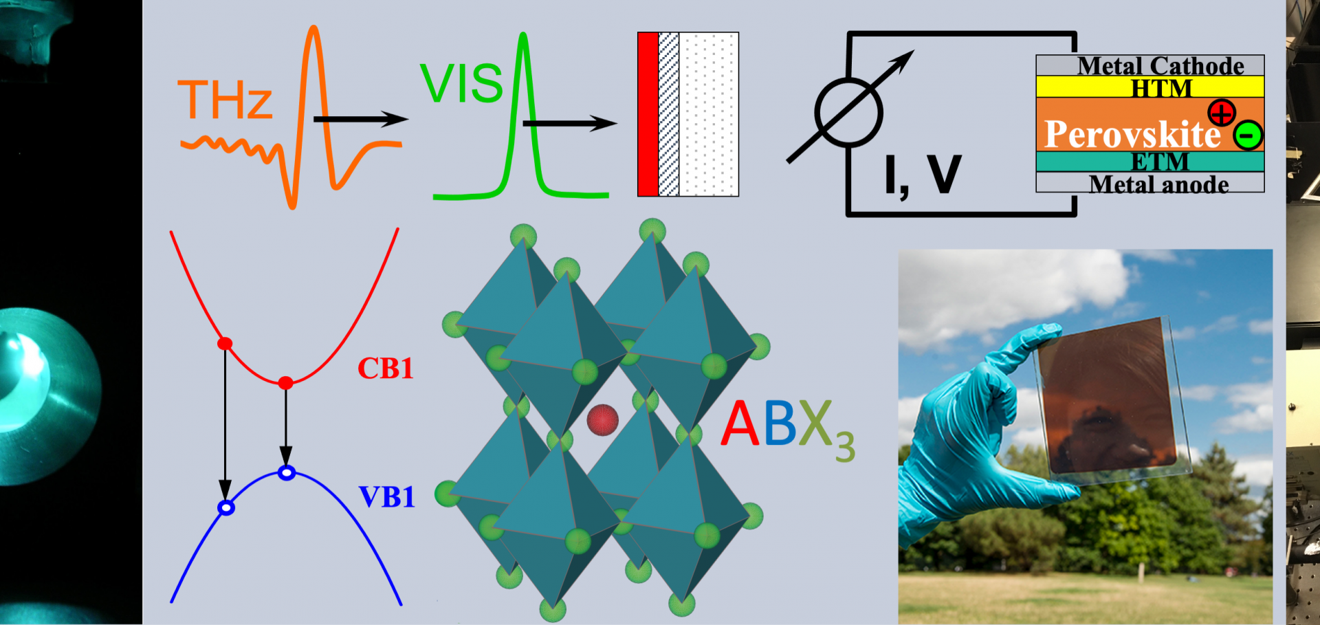
Abstract:
Halogen mixing in lead-halide perovskites is an effective route for tuning the band gap in light emission and multijunction solar cell applications. Here we report the effect of halogen mixing on the optoelectronic properties of lead-halide perovskites from theory and experiment. We applied the virtual crystal approximation within density functional theory, the <i>GW</i> approximation, and the Bethe-Salpeter equation to calculate structural, vibrational, and optoelectronic properties for a series of mixed halide perovskites. We separately perform spectroscopic measurements of these properties and analyze the impact of halogen mixing on quasiparticle band gaps, effective masses, absorption coefficients, charge-carrier mobilities, and exciton binding energies. Our joint theoretical-experimental study demonstrates that iodide-bromide mixed-halide perovskites can be modeled as homovalent alloys, and local structural distortions do not play a significant role for the properties of these mixed species. Our study outlines a general theoretical-experimental framework for future investigations of novel chemically mixed systems.Time-resolved vibrational-pump visible-probe spectroscopy for thermal conductivity measurement of metal-halide perovskites.
The Review of scientific instruments 93:5 (2022) 053003
Abstract:
Understanding thermal transport at the microscale to the nanoscale is crucially important for a wide range of technologies ranging from device thermal management and protection systems to thermal-energy regulation and harvesting. In the past decades, non-contact optical methods, such as time-domain and frequency-domain thermoreflectance, have emerged as extremely powerful and versatile thermal metrological techniques for the measurement of material thermal conductivities. Here, we report the measurement of thermal conductivity of thin films of CH3NH3PbI3 (MAPbI3), a prototypical metal-halide perovskite, by developing a time-resolved optical technique called vibrational-pump visible-probe (VPVP) spectroscopy. The VPVP technique relies on the direct thermal excitation of MAPbI3 by femtosecond mid-infrared optical pump pulses that are wavelength-tuned to a vibrational mode of the material, after which the time dependent optical transmittance across the visible range is probed in the ns to the μs time window using a broadband pulsed laser. Using the VPVP method, we determine the thermal conductivities of MAPbI3 thin films deposited on different substrates. The transducer-free VPVP method reported here is expected to permit spectrally resolving and spatiotemporally imaging of the dynamic lattice temperature variations in organic, polymeric, and hybrid organic-inorganic semiconductors.Silver-Bismuth based 2D Double Perovskites (4FPEA)4AgBiX8 (X=Cl, Br, I): Highly Oriented Thin Films with Large Domain Sizes and Ultrafast Charge-Carrier Localization
Fundacio Scito (2022)
Triple-Source Co-evaporation of lead-free Cu2AgBiI6 for Use in Tandem Solar Cells
Fundacio Scito (2022)
Defect Etching in Carbon Nanotube Walls for Porous Carbon Nanoreactors: Implications for CO2 Sorption and the Hydrosilylation of Phenylacetylene
ACS Applied Nano Materials American Chemical Society (ACS) 5:2 (2022) 2075-2086