

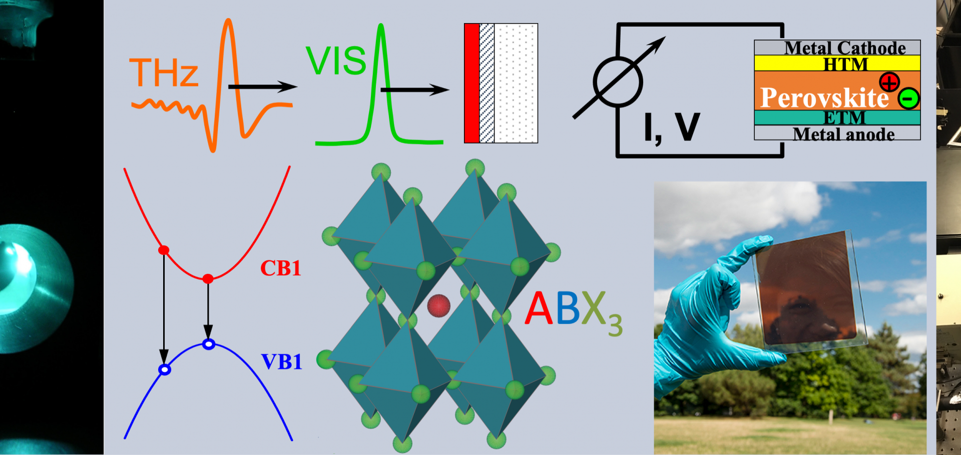
A green solvent system for templated sequential deposition of stable formamidinium lead triiodide for perovskite solar cells
Photophysics and structural dynamics in metal-halide perovskite semiconductors
Abstract:
Metal-halide perovskites have been under intense research over the past decade due to their potential to compete with and complement silicon in solar photovoltaic devices, owing to their affordability and better device performances. However, their commercialisation has been hindered mainly due to their problems with stability, which requires more thorough fundamental investigation of these materials. This thesis focuses on understanding their photophysics and structural dynamics through various spectroscopic techniques. More specifically, metal-halide perovskites have issues regarding halide segregation and tin oxidation, as well as intriguing low-frequency Raman response, which are addressed in this thesis.
The effects of a hole-transport layer and defect passivation on halide segregation under illumination in mixed-halide perovskites have been investigated using in-situ photoluminescence and X-ray diffraction. It is demonstrated that using photoluminescence on its own may be misleading when studying halide segregation, especially when a charge-transport layer is present. The introduction of a hole-transport layer slows down halide segregation due to hole depletion, but increases the photoluminescence intensity through hole back-transfer into iodide-rich regions near the interface between the perovskite and the hole-transport layer. It is shown that defect passivation has a profound and complex effect on halide segregation, and the nature of the trap states determines their role in halide segregation.The degradation mechanisms in tin-only and mixed lead-tin iodide perovskites in ambient air have been examined. Although these two different types of perovskites both undergo severe optoelectronic degradation in ambient air over a few hours, their degradation mechanisms have been shown to differ; tin-only perovskites undergo heavy doping of the valence band when exposed to ambient air, but mixed lead-tin perovskites do not undergo any significant doping during exposure. It was concluded that tin-only perovskites degrade via introduction of shallow defect states which contribute to hole-doping of the valence band, while mixed lead-tin perovskites degrade via formation of deep trap states which do not significantly dope either of the electronic bands. Possible degradation products during ambient air exposure of these perovskites have also been identified.
Finally, low-frequency vibrational properties of metal-halide perovskites were investigated. Metal-halide perovskites have been reported to have intriguing responses in low-frequency Raman spectra, where the response is extremely broad. However, this is not the case for IR spectra, where only well-defined contribution from phonon modes are visible. The origin of the broad Raman response, as well as the discrepancy between Raman and IR spectra, has been an actively debated topic in the literature, with various hypotheses being presented. Through Raman and IR spectra of various metal-halide semiconductors and literature data, a number of hypotheses have been ruled out as the main cause of such Raman response. Those that are ruled out include: extrinsic defects, octahedral tilting, cation lone pairs, and ‘liquid-like’ Boson peaks. Instead, an alternative explanation for such broad Raman response and the discrepancy with IR spectra was presented: the broad Raman response is a result of an interplay of significant broadening of Raman-active vibrational modes and a Bose-Einstein population factor, while IR-active vibrational modes are subject to different and slower decay channels, and such Bose-Einstein population factor is not applicable to IR spectra.
Photophysics at interfaces between metal-halide semiconductors and charge-transport layers
Abstract:
Metal-halide semiconductors have emerged as promising materials for solar cells, with lead-based perovskites demonstrating remarkable efficiencies in tandem architectures. Yet, their performance still falls short of the theoretical limit, especially for wide-bandgap semiconductors, primarily due to interfacial losses at the semiconductor/charge-transport layer interface. This thesis investigates the photophysics at these interfaces through various spectroscopic techniques, providing insights into the underlying loss mechanisms and guiding mitigating strategies to achieve higher efficiencies.Unfavourable energy-level alignment at the interface with charge-transport layers results in substantial open-circuit voltage losses. A systematic increase in the valence band maximum of FA0.83Cs0.17Pb (I1−𝑥Br𝑥 )3 with increasing bromide content 𝑥 from 0 to 1, when interfaced with the commonly employed hole transport layer poly[bis(4-phenyl)(2,4,6-trimethylphenyl)amine] (PTAA), provides an ideal platform to study photophysical losses arising from energy-level misalignment. The combination of time-resolved photoluminescence and numerical modeling reveals that increasing energy-level misalignment leads to increasing accumulation of holes in PTAA, which then subsequently recombine non-radiatively across the interface via interfacial defects, thereby reducing the open-circuit voltage and overall device efficiency.
Wide-bandgap mixed-halide perovskites often suffer from halide segregation where prolonged illumination drives a spatial separation of the mixed-phase perovskite into both iodide-rich (I-rich) and bromide-rich domains. By using a synchronous multimodal spectroscopy that combines timeresolved photoluminescence, time-resolved microwave conductivity and steady-state photoluminescence spectroscopy, the effect of halide segregation on the interfacial processes at FA0.83Cs0.17Pb(I0.6Br0.4 )3 interfaced with commonly used charge-transport layers such as PTAA and SnO2 is investigated. In neat perovskite films, halide segregation enhances radiative bimolecular recombination as charge-carrier funnelling increases the local carrier density within the narrow bandgap I-rich domains. Nevertheless, the charge-carrier mobility remains largely preserved after segregation. In the presence of charge-transport layers, charge extraction occurs predominantly via the I-rich phase following segregation. Although mobility retention is reduced in these heterostructures, the transport layers facilitate charge back transfer, mitigating the reduction in carrier lifetime at later times. The combined decrease in lifetime owing to enhanced radiative recombination and reduction in mobilities limits the diffusion length and therefore charge-carrier collection efficiency after halide segregation.
Concerns over the lead toxicity and instability of metal-halide perovskites have motivated the development of lead-free, all-inorganic Cu2AgBiI6 within the CuI–AgI–BiI3 phase space. However, it suffers from lower device efficiencies compared to its lead-perovskite counterparts, primarily due to poor charge-collection efficiency. Optoelectronic studies of coevaporated Cu2AgBiI6 interfaced with various charge-transport layers such as PTAA, CuI, [6,6]-phenyl-C61-butyric acid methyl ester (PCBM) and SnO2 revealed that inorganic transport layers such as CuI and SnO2 induce the formation of unintended impurity phases within the CuI–AgI–BiI3 phase space, significantly altering structural and optoelectronic properties. These impurities reduce charge-carrier mobilities and diffusion lengths, thereby limiting its device efficiency.