
Nanowires: A New Horizon for Polarization-resolved Terahertz Time-domain Spectroscopy
2021 Conference on Lasers and Electro-Optics, CLEO 2021 - Proceedings (2021)
Abstract:
In this study, a novel type of broadband polarization-sensitive photoconductive terahertz detectors based on crossed nanowire networks is demonstrated, enabling fast and precise polarization terahertz time-domain spectroscopy measurements.Charge-carrier mobility and localization in semiconducting CU2AGBiI6 for photovoltaic applications
ACS Energy Letters American Chemical Society 6:5 (2021) 1729-1739
Abstract:
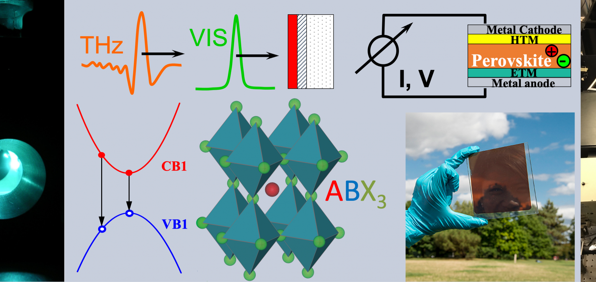
Lead-free silver–bismuth semiconductors have become increasingly popular materials for optoelectronic applications, building upon the success of lead halide perovskites. In these materials, charge-lattice couplings fundamentally determine charge transport, critically affecting device performance. In this study, we investigate the optoelectronic properties of the recently discovered lead-free semiconductor Cu2AgBiI6 using temperature-dependent photoluminescence, absorption, and optical-pump terahertz-probe spectroscopy. We report ultrafast charge-carrier localization effects, evident from sharp THz photoconductivity decays occurring within a few picoseconds after excitation and a rise in intensity with decreasing temperature of long-lived, highly Stokes-shifted photoluminescence. We conclude that charge carriers in Cu2AgBiI6 are subject to strong charge-lattice coupling. However, such small polarons still exhibit mobilities in excess of 1 cm2 V–1 s–1 at room temperature because of low energetic barriers to formation and transport. Together with a low exciton binding energy of ∼29 meV and a direct band gap near 2.1 eV, these findings highlight Cu2AgBiI6 as an attractive lead-free material for photovoltaic applications.Limits to electrical mobility in lead-halide perovskite semiconductors
Journal of Physical Chemistry Letters American Chemical Society 12:14 (2021) 3607-3617
Abstract:
Semiconducting polycrystalline thin films are cheap to produce and can be deposited on flexible substrates, yet high-performance electronic devices usually utilize single-crystal semiconductors, owing to their superior charge-carrier mobilities and longer diffusion lengths. Here we show that the electrical performance of polycrystalline films of metal-halide perovskites (MHPs) approaches that of single crystals at room temperature. Combining temperature-dependent terahertz conductivity measurements and ab initio calculations we uncover a complete picture of the origins of charge-carrier scattering in single crystals and polycrystalline films of CH3NH3PbI3. We show that Fröhlich scattering of charge carriers with multiple phonon modes is the dominant mechanism limiting mobility, with grain-boundary scattering further reducing mobility in polycrystalline films. We reconcile the large discrepancy in charge-carrier diffusion lengths between single crystals and films by considering photon reabsorption. Thus, polycrystalline films of MHPs offer great promise for devices beyond solar cells, including light-emitting diodes and modulators.Ultrafast excited-state localization in Cs2AgBiBr6 double perovskite
Journal of Physical Chemistry Letters American Chemical Society 12:13 (2021) 3352-3360
Abstract:
Cs2AgBiBr6 is a promising metal halide double perovskite offering the possibility of efficient photovoltaic devices based on lead-free materials. Here, we report on the evolution of photoexcited charge carriers in Cs2AgBiBr6 using a combination of temperature-dependent photoluminescence, absorption and optical pump–terahertz probe spectroscopy. We observe rapid decays in terahertz photoconductivity transients that reveal an ultrafast, barrier-free localization of free carriers on the time scale of 1.0 ps to an intrinsic small polaronic state. While the initially photogenerated delocalized charge carriers show bandlike transport, the self-trapped, small polaronic state exhibits temperature-activated mobilities, allowing the mobilities of both to still exceed 1 cm2 V–1 s–1 at room temperature. Self-trapped charge carriers subsequently diffuse to color centers, causing broad emission that is strongly red-shifted from a direct band edge whose band gap and associated exciton binding energy shrink with increasing temperature in a correlated manner. Overall, our observations suggest that strong electron–phonon coupling in this material induces rapid charge-carrier localization.Unveiling the ultrafast optoelectronic properties of 3D Dirac semi-metal Cd3As2
Proceedings of the 45th International Conference on Infrared, Millimeter, and Terahertz Waves (IRMMW-THz 2020) IEEE (2021)