Is Photoluminescence Spectroscopy a Suitable Probe of Halide Segregation?
ACS Energy Letters American Chemical Society (ACS) (2026) acsenergylett.6c00432
Halide segregation governs interfacial charge-transfer pathways in mixed-halide perovskites
EES Solar Royal Society of Chemistry (2026)
Abstract:
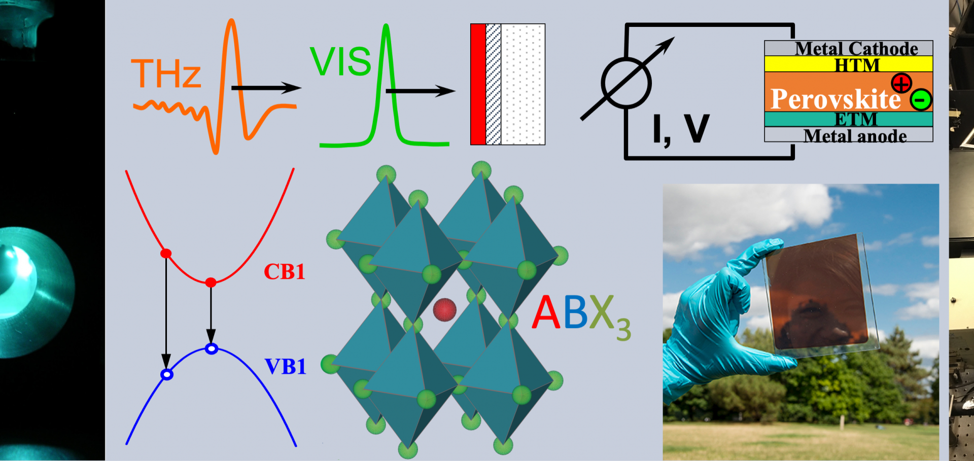
Mixed-halide perovskites offer ideal bandgaps for tandem solar cells, but they suffer from light-induced halide segregation, which compromises their operational stability. Here, we directly probe the impact of halide segregation on charge-carrier dynamics at the interface between a mixed-halide perovskite and charge transport layers by using a free-space synchronous multimodal spectroscopy approach, combining time-resolved microwave conductivity, time-resolved photoluminescence (PL) and steady-state PL. We present a method to distinguish directly between charge-carrier dynamics dominated by either majority or minority carriers, enabling us to isolate effects arising from charge-selective extraction from the perovskite to commonly used hole- or electron transport layers, i.e. poly[bis(4-phenyl)(2,4,6-trimethylphenyl)amine] (PTAA) and SnO2, respectively. We show that halide segregation creates iodide-rich phases that capture charge carriers within sub-nanoseconds, which slightly reduces their mobilities at microwave frequencies. We reveal that charge extraction from such iodide-rich domains is still surprisingly feasible, but competes with enhanced radiative recombination resulting from higher charge concentrations caused by funnelling into these minority phases. We demonstrate that together such effects reduce charge diffusion lengths and can account for the widely observed reduction in open-circuit voltages and short-circuit currents in solar cells under operational conditions. Our findings unravel the causes underpinning the adverse impact of halide segregation and provide guidelines to improve device performance.Impact of residual triphenylphosphine oxide on the crystallization of vapor-deposited metal halide perovskite films
Journal of Vacuum Science & Technology B Nanotechnology and Microelectronics Materials Processing Measurement and Phenomena American Vacuum Society 44:1 (2026) 012203
Abstract:
Thermal evaporation is an industrially compatible technique for fabricating metal halide perovskite thin films, without the requirement for hazardous solvents. It offers precise control over film thickness and is a good candidate for large-scale production of commercial optoelectronic metal halide perovskite devices, such as solar cells. The use of additives to passivate electronic defects in solution-processed metal halide perovskite has led to dramatic increases in device performance. However, there are a few reports of vapor-deposited films with coevaporated passivating agents. Triphenylphosphine oxide (TPPO) has been used as an effective surface passivating agent in solution-processed metal halide perovskite films. It is a promising candidate passivating agent for coevaporation, where it is beginning to be used with encouraging results. However, here we report that triphenylphosphine oxide is incompatible with thermal deposition in the same deposition chamber. Such TPPO remnants are found to result in severe suppression of the perovskite phase, long-range crystalline ordering, and optical absorption of lead halide perovskite films subsequently deposited in the same chamber. TPPO contamination persists even through repeated baking cycles, with the reduction of the contaminant to acceptable levels requiring vacuum chamber dismantling and manual cleaning. We conclude that TPPO should not be coevaporated in order to prevent the contamination of future batches.Discovery of two new Cu–Sn chalco–halides for potential solar absorber applications
Journal of Materials Chemistry A Royal Society of Chemistry (RSC) (2026)
Abstract:
New compounds are discovered in the under-explored d 10 –s 2 (Cu–Sn) family using exploratory synthesis guided by computational tools. Band-gaps in the visible region with moderate charge-carrier mobilities make these potential solar absorbers. We explore multiple-cation chalco–halide phase fields evaluated by their synthetic accessibility using machine learning models. Exploratory synthesis guided by computational tools leads to the discovery of two new compounds; CuSn 2 SI 3 and Cu 0.35 Sn 5.29 S 2 I 7 , their structures, and electronic and optical properties are reported herein. This is the first report of a stable quaternary compound in the Cu–Sn–S–I phase field. The two new compounds show related crystal structures where Sn 4 S 2 I 4 layers are a common structural motif in both. These Sn 4 S 2 I 4 layers are connected by Cu 2 I 2 layers and disordered Cu–Sn–I layers, forming the three-dimensional structures of CuSn 2 SI 3 and Cu 0.35 Sn 5.29 S 2 I 7 respectively. Electronic band structure calculations using density functional theory show the presence of a direct band gap in CuSn 2 SI 3 and suggest anisotropic transport, in line with the layered structure of the compound. A mixture of the two compounds with ∼86% CuSn 2 SI 3 , shows a band gap in the visible region, close to 2.1 eV and a significant photo-induced charge carrier mobility of ∼1.3 cm 2 V −1 s −1 . This demonstrates Cu–Sn chalco–halides can form a promising phase space to explore for solar absorber materials, with further design and tuning of band gap.Perovskite‐based time‐domain signal‐balancing LiDAR sensor with centimeter depth resolution
InfoMat Wiley (2025) e70104


