
Crystallization of CsPbBr3 single crystals in water for X-ray detection
Nature Communications Springer Nature 12:1 (2021) 1531
Highly absorbing lead-free semiconductor Cu2AgBiI6 for photovoltaic applications from the quaternary CuI-AgI-BiI3 phase space
Journal of the American Chemical Society American Chemical Society 143:10 (2021) 3983-3992
Abstract:
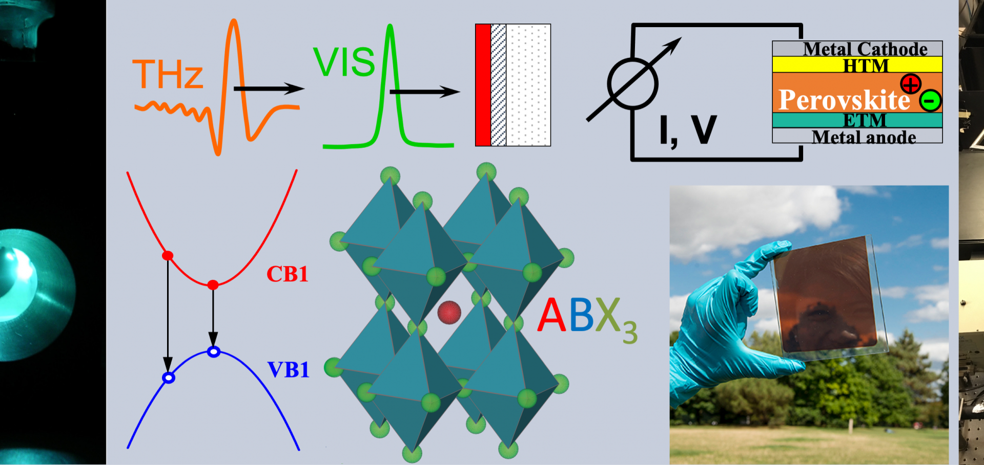
Since the emergence of lead halide perovskites for photovoltaic research, there has been mounting effort in the search for alternative compounds with improved or complementary physical, chemical, or optoelectronic properties. Here, we report the discovery of Cu2AgBiI6: a stable, inorganic, lead-free wide-band-gap semiconductor, well suited for use in lead-free tandem photovoltaics. We measure a very high absorption coefficient of 1.0 × 105 cm–1 near the absorption onset, several times that of CH3NH3PbI3. Solution-processed Cu2AgBiI6 thin films show a direct band gap of 2.06(1) eV, an exciton binding energy of 25 meV, a substantial charge-carrier mobility (1.7 cm2 V–1 s–1), a long photoluminescence lifetime (33 ns), and a relatively small Stokes shift between absorption and emission. Crucially, we solve the structure of the first quaternary compound in the phase space among CuI, AgI and BiI3. The structure includes both tetrahedral and octahedral species which are open to compositional tuning and chemical substitution to further enhance properties. Since the proposed double-perovskite Cs2AgBiI6 thin films have not been synthesized to date, Cu2AgBiI6 is a valuable example of a stable Ag+/Bi3+ octahedral motif in a close-packed iodide sublattice that is accessed via the enhanced chemical diversity of the quaternary phase space.Halide segregation in mixed-halide perovskites: influence of A-site cations
ACS Energy Letters American Chemical Society 6:2 (2021) 799-808
Abstract:
Mixed-halide perovskites offer bandgap tunability essential for multijunction solar cells; however, a detrimental halide segregation under light is often observed. Here we combine simultaneous in situ photoluminescence and X-ray diffraction measurements to demonstrate clear differences in compositional and optoelectronic changes associated with halide segregation in MAPb(Br0.5I0.5)3 and FA0.83Cs0.17Pb(Br0.4I0.6)3 films. We report evidence for low-barrier ionic pathways in MAPb(Br0.5I0.5)3, which allow for the rearrangement of halide ions in localized volumes of perovskite without significant compositional changes to the bulk material. In contrast, FA0.83Cs0.17Pb(Br0.4I0.6)3 lacks such low-barrier ionic pathways and is, consequently, more stable against halide segregation. However, under prolonged illumination, it exhibits a considerable ionic rearrangement throughout the bulk material, which may be triggered by an initial demixing of A-site cations, altering the composition of the bulk perovskite and reducing its stability against halide segregation. Our work elucidates links between composition, ionic pathways, and halide segregation, and it facilitates the future engineering of phase-stable mixed-halide perovskites.Terahertz full-polarization-state detection by nanowires
Optics InfoBase Conference Papers (2021)
Terahertz full-polarization-state detection by nanowires
Optics InfoBase Conference Papers (2021)