Observation of nodal line in non-symmorphic topological semimetal InBi
New Journal of Physics IOP Publishing 19:065007 (2017) 1-8
Abstract:
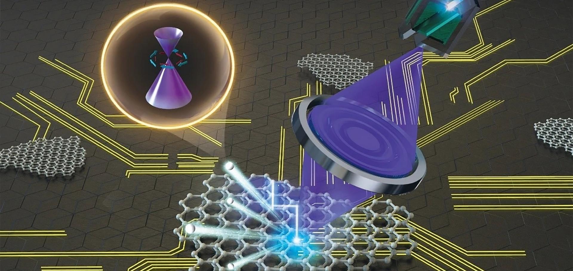
Topological nodal semimetal (TNS), characterized by its touching conduction and valence bands, is a newly discovered state of quantum matter which exhibits various exotic physical phenomena. Recently, a new type of TNS called topological nodal line semimetal (TNLS) is predicted where its conduction and valence band form a degenerate one-dimension line which is further protected by its crystal symmetry. In this work, we systematically investigated the bulk and surface electronic structure of the non-symmorphic, TNLS in InBi (which is also a type II Dirac semimetal) with strong spin-orbit coupling by using angle resolved photoemission spectroscopy. By tracking the crossing points of the bulk bands at the Brillouin zone boundary, we discovered the nodal-line feature along the kz direction, in agreement with the ab initio calculations and confirmed it to be a new compound in the TNLS family. Our discovery provides a new material platform for the study of these exotic topological quantum phases and paves the way for possible future applications.Emergence of Dirac-like bands in the monolayer limit of epitaxial Ge films on Au(1 1 1)
2D Materials Institute of Physics 4:3 (2017) 031005
Abstract:
After the discovery of Dirac fermions in graphene, it has become a natural question to ask whether it is possible to realize Dirac fermions in other two-dimensional (2D) materials as well. In this work, we report the discovery of multiple Dirac-like electronic bands in ultrathin Ge films grown on Au(1 1 1) by angle-resolved photoelectron spectroscopy. By tuning the thickness of the films, we are able to observe the evolution of their electronic structure when passing through the monolayer limit. Our discovery may signify the synthesis of germanene, a 2D honeycomb structure made of Ge, which is a promising platform for exploring exotic topological phenomena and enabling potential applications.Nontrivial Berry phase and type-II Dirac transport in the layered material PdTe2
Physical Review B American Physical Society (APS) 96:4 (2017) 041201
Quantum spin Hall state in monolayer 1T'-WTe2
Nature Physics Springer Nature 13:7 (2017) 683-687
Substrate Doping Effect and Unusually Large Angle van Hove Singularity Evolution in Twisted Bi‐ and Multilayer Graphene
Advanced Materials Wiley 29:27 (2017)