Modulating lattice strain and defect formation in halide perovskites
Supervisors: Prof. Nakita Noel (Physics) and Prof. Saiful Islam (Materials)
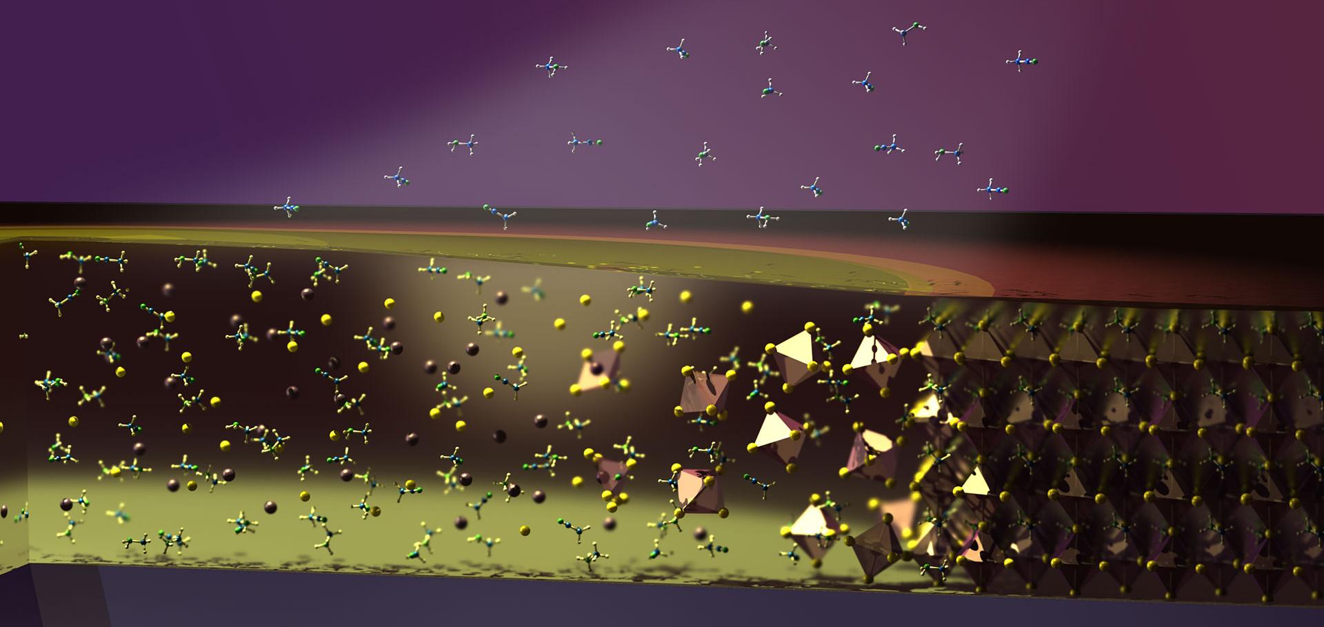
This project addresses a key challenge in the field of photovoltaic materials science: developing not just efficient, but stable halide perovskite solar cells for sustainable energy generation. The research will focus on understanding and controlling the structural and chemical factors that govern lattice strain and defect formation in perovskite thin films. By integrating synthesis, advanced structural and spectroscopic characterisation, and computational modelling with machine learning, the project aims to establish new chemical routes for modulating lattice properties and improving long-term device stability. This interdisciplinary approach will provide fundamental insights into the relationship between composition, structure, and optoelectronic performance in perovskite semiconductors.
The successful applicant will gain training in materials synthesis, diffraction and electron microscopy, photophysical measurements, and computational materials analysis. The project will explore mechanisms such as ion migration and the role of structure directing additives in thin-film crystal growth and material stability. Results will directly inform the design of stable perovskite layers for single-junction and multijunction solar cells, making an essential step towards scalable, low-cost renewable energy technologies.
Development of stable wide-bandgap perovskites for silicon-based tandem solar cells
Perovskite solar cells have emerged as a key enabler for ultra-high-efficiency tandem solar cell technology. Perovskite semiconductors can be produced using low-cost, high throughput, and sustainable techniques, already demonstrating solar cells with remarkable (>26%) power conversion efficiencies (PCEs). When combined with silicon in a tandem configuration, they can surpass the efficiency limits of single-junction silicon cells (29%), potentially reaching PCEs > 40%, and driving solar power to the lowest levelized cost of electricity in many places around the world.
Perovskites can be engineered to have various bandgaps, making them highly versatile for tandem integration and allowing for optimised cell configurations that maximise efficiency. Perovskites and silicon have complementary absorption characteristics where silicon cells efficiently convert red and infrared light, while perovskites are highly effective at absorbing blue and green light. By stacking a perovskite on top of a silicon cell, tandem devices can exploit a broader range of the solar spectrum, leading to higher energy conversion. Overall, perovskite-silicon tandems represent a promising avenue for achieving higher efficiencies and lower costs in solar energy, accelerating the adoption of renewable energy technologies worldwide.
Recent work has shown that the synthetic routes to fabricate hybrid (inorganic-organic) perovskite materials can be influenced by cation additives which can control intermediate precursor phases, and result in material with enhanced stability. Additives can help precisely tune the material composition, grain size, orientation, and crystallinity in hybrid perovskite systems. Such approaches are yet to be brought to the top of a silicon solar cell to assemble a tandem, since the textured surface of silicon creates an additional barrier to material synthesis. This project will involve the development of new synthetic routes to manufacture perovskite semiconductors based on additives. Manufactured materials will be characterised to obtain the nanostructure (diffraction and electron microscopy) and optoelectronic properties (luminescence, current-voltage, spectroscopy). Devices will then be fabricated, measured, and modelled, aiming to demonstrate highly stable materials on a pyramidally textured silicon solar cell.
Advanced Device Concepts for Next-Generation Photovoltaics
A number of fully funded studentship projects are available and will be associated with an exciting new EPSRC/UKRI-funded Programme Grant, a collaborative project that brings together expertise in photovoltaic materials synthesis and device fabrication, advanced characterisation and modelling. The ambition for this project is to carry out multidisciplinary research, via inter-linked work streams, that will explore and conceive four new photovoltaic device concepts and paradigms, enabling the next major step-change in photovoltaic efficiency. New devices architectures, concentrator PV, quantum cutting, hot-carrier collection and photon transport, will be explored and enabled by absorber materials based on metal-halide perovskites, silicon, and novel low-band-gap chalcogenide-halide semiconductors, supported by fundamental experimental characterisation and materials modelling. Addressing these future advanced concepts through a holistic approach will enable key scientific discoveries and important major technical advances enabling the next generation of PV technologies for beyond 2030.
Applicants for DPhil studentships are invited to choose amongst projects focusing on the following areas:
Design, synthesis and discovery of new inorganic semiconductors with new optoelectronic functionality
Projects will focus on the synthesis, processing and characterisation of novel semiconductors for optoelectronic applications
Advanced experimental characterisation
Projects will focus on the use of advanced electron imaging and diffraction techniques to understand the impact of nanoscale structure on optoelectronic properties
To be considered, applicants must apply for a “DPhil in Condensed Matter Physics” through the University’s online portal (DPhil in Condensed Matter Physics | University of Oxford) and state the above project title and preferred supervisor(s) on their application.
Improving halide perovskite photovoltaic performance by understanding how structure and local composition control properties
Supervisors: Prof. Nakita Noel (Physics) and Prof. Pete Nellist (Materials)
Within the last decade, halide perovskites have become one of the most ubiquitous materials in optoelectronics research. Due to their impressive optoelectronic properties-long diffusion lengths, high carrier mobilities and broad, tunable absorption, these materials are currently the front runners in emerging thin-film photovoltaics. While the efficiencies of perovskite photovoltaics (>26%) and light emitting diodes have soared, there are still fundamental questions about the structure-property relationships which exist in these materials that remain unanswered. This overarching goal of this project is to use high-resolution electron microscopy to conduct a detailed investigation into the nanoscale structure/composition of halide perovskite materials and relate this to their (i) optoelectronic properties and (ii) device performance. This includes but is not necessarily limited to the investigation of typical 3D perovskite structures, so-called hollow perovskites, and the interfaces of halide perovskites and charge transport layers. The project will make use of thin-film material processing and characterisation equipment in the Physics department, and of a recently installed STEM/TEM with a number of novel features to allow investigation of beam sensitive materials, including flexible beam intensity control, cryo-fins to reducing icing on sample cooling, high solid-angle EDX spectroscopy and EELS in the Materials department.
The impact of crystallisation kinetics on the stability and optoelectronic performance of halide perovskites
Lead halide perovskites are particularly promising candidates for integration into high performance photovoltaic devices. As this technology moves closer to commercialisation, a fundamental understanding of the growth mechanisms underlying high performance, and importantly, high-stability perovskite thin-films must be achieved. This project aims to establish a deeper understanding of the transformation from precursor materials to high-quality perovskite thin films, mapping conversion processes and defect formation using a combination of chemical, structural and spectroscopic investigations. This will also allow for probing the impact of altering kinetic pathways on the thermodynamic stability perovskite thin-films with the most promising materials being integrated into high-performance photovoltaic or light-emitting devices.