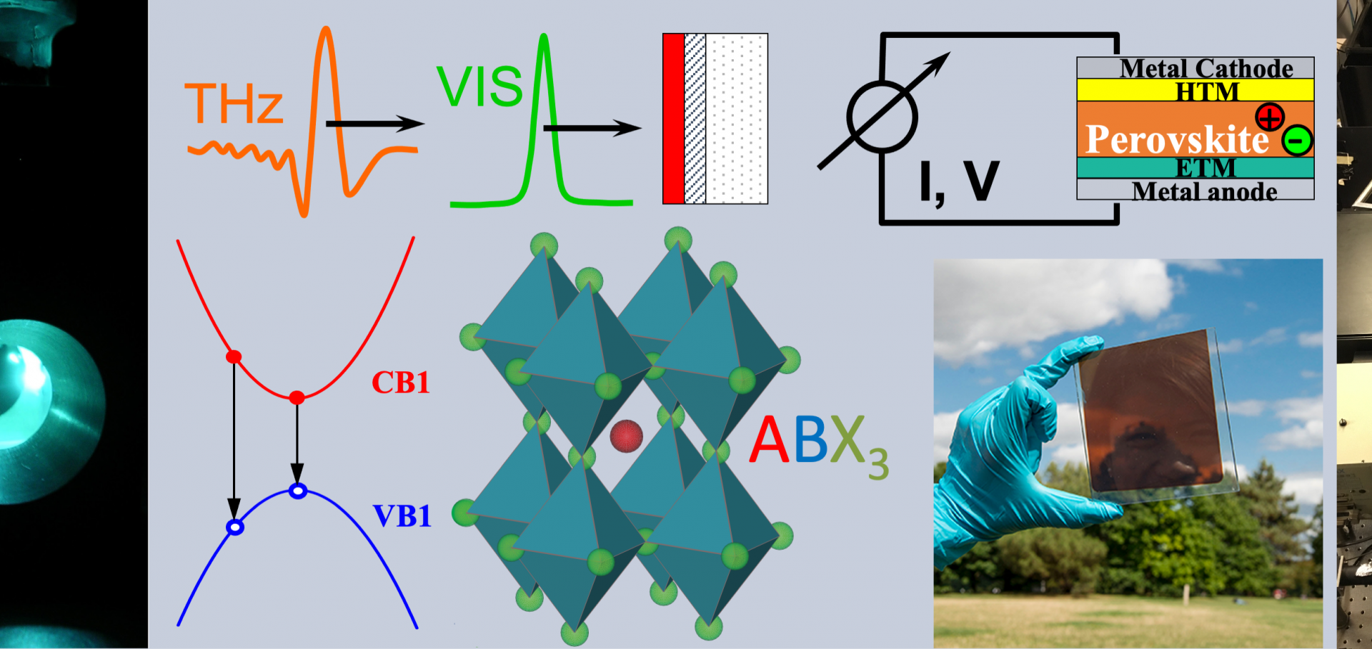
Modulating non-radiative recombination related to shallow traps in halide perovskites
Applied Physics Reviews 13:1 (2026)
Abstract:
Halide perovskite solar cells have demonstrated a rapid increase in power conversion efficiencies. Understanding and mitigating remaining carrier losses in halide perovskites is now crucial to enable further increases to approach their practical efficiency limits. Recent observations in halide perovskites have revealed processes such as shallow carrier trapping, which give rise to an apparent non-radiative bimolecular channel that is difficult to distinguish from intrinsic radiative recombination. Here, we quantify this shallow-trap manifestation by jointly analyzing time-resolved photoluminescence and quantum efficiency to separate the total second-order term into radiative (ηImpact of residual triphenylphosphine oxide on the crystallization of vapor-deposited metal halide perovskite films
Journal of Vacuum Science & Technology B Nanotechnology and Microelectronics Materials Processing Measurement and Phenomena American Vacuum Society 44:1 (2026) 012203
Abstract:
Thermal evaporation is an industrially compatible technique for fabricating metal halide perovskite thin films, without the requirement for hazardous solvents. It offers precise control over film thickness and is a good candidate for large-scale production of commercial optoelectronic metal halide perovskite devices, such as solar cells. The use of additives to passivate electronic defects in solution-processed metal halide perovskite has led to dramatic increases in device performance. However, there are a few reports of vapor-deposited films with coevaporated passivating agents. Triphenylphosphine oxide (TPPO) has been used as an effective surface passivating agent in solution-processed metal halide perovskite films. It is a promising candidate passivating agent for coevaporation, where it is beginning to be used with encouraging results. However, here we report that triphenylphosphine oxide is incompatible with thermal deposition in the same deposition chamber. Such TPPO remnants are found to result in severe suppression of the perovskite phase, long-range crystalline ordering, and optical absorption of lead halide perovskite films subsequently deposited in the same chamber. TPPO contamination persists even through repeated baking cycles, with the reduction of the contaminant to acceptable levels requiring vacuum chamber dismantling and manual cleaning. We conclude that TPPO should not be coevaporated in order to prevent the contamination of future batches.Discovery of two new Cu–Sn chalco–halides for potential solar absorber applications
Journal of Materials Chemistry A Royal Society of Chemistry (RSC) (2026)
Abstract:
New compounds are discovered in the under-explored d 10 –s 2 (Cu–Sn) family using exploratory synthesis guided by computational tools. Band-gaps in the visible region with moderate charge-carrier mobilities make these potential solar absorbers. We explore multiple-cation chalco–halide phase fields evaluated by their synthetic accessibility using machine learning models. Exploratory synthesis guided by computational tools leads to the discovery of two new compounds; CuSn 2 SI 3 and Cu 0.35 Sn 5.29 S 2 I 7 , their structures, and electronic and optical properties are reported herein. This is the first report of a stable quaternary compound in the Cu–Sn–S–I phase field. The two new compounds show related crystal structures where Sn 4 S 2 I 4 layers are a common structural motif in both. These Sn 4 S 2 I 4 layers are connected by Cu 2 I 2 layers and disordered Cu–Sn–I layers, forming the three-dimensional structures of CuSn 2 SI 3 and Cu 0.35 Sn 5.29 S 2 I 7 respectively. Electronic band structure calculations using density functional theory show the presence of a direct band gap in CuSn 2 SI 3 and suggest anisotropic transport, in line with the layered structure of the compound. A mixture of the two compounds with ∼86% CuSn 2 SI 3 , shows a band gap in the visible region, close to 2.1 eV and a significant photo-induced charge carrier mobility of ∼1.3 cm 2 V −1 s −1 . This demonstrates Cu–Sn chalco–halides can form a promising phase space to explore for solar absorber materials, with further design and tuning of band gap.Decoupling Optical and Thermal Dynamics in Dielectric Metasurfaces for Self-Encoded Photonic Control
Laser and Photonics Reviews 19:24 (2025)
Abstract:
Thermo-optical nonlinearities (TONL) in metasurfaces enable dynamic control of optical properties—such as transmitted power, phase, and polarization—through external stimuli like laser irradiation or temperature. Due to the inherently slow thermal dynamics of extended systems, research has primarily focused on steady-state effects, as rapid modulation is typically considered challenging. In this study, photo-driven TONL is investigated in amorphous silicon (a-Si) metasurfaces under both steady-state and, more importantly, dynamic conditions using a modulated 488 nm continuous-wave pump laser. First, a non-monotonic change is observed in transmission as a function of irradiation intensity at a wavelength red-shifted by 15 nm from the electric-dipole resonance. Specifically, transmission initially decreases by 30% before increasing by 30% as the laser intensity reaches 5 mW/ (Formula presented.). Next, it is demonstrated that TONL decouple thermal and optical response times, with the optical response being up to seven times faster than the thermal response under tested conditions ((Formula presented.) (Formula presented.) vs. (Formula presented.) (Formula presented.)). Most remarkably, it is experimentally shown that the interplay of these effects enables optical modulation at twice (100 kHz) the excitation laser's modulation frequency (50 kHz). Finally, it is shown that exploiting these unique conditions allow thermo-optical metasurfaces to intrinsically encode multiple optical states within a single modulation cycle, realizing a self-modulating photonic platform. TONL thus open new avenues for engineering active metasurfaces that combine fast, high-amplitude modulation with self-modulating optical dynamics, making them promising for next-generation optical switching, dynamic holography, optical information processing, and neuromorphic computing.Inter-Layer Diffusion of Excitations in 2D Perovskites Revealed by Photoluminescence Reabsorption
Fundacio Scito (2025)