Linking Surface Chemistry to Phonon and Carrier Dynamics in CsPbBr3 Nanocrystals
Fundacio Scito (2025)
Overcoming Charge-Carrier Localisation in Metal Chalcohalides
Fundacio Scito (2025)
Perovskite‐based time‐domain signal‐balancing LiDAR sensor with centimeter depth resolution
InfoMat Wiley (2025) e70104
Abstract:
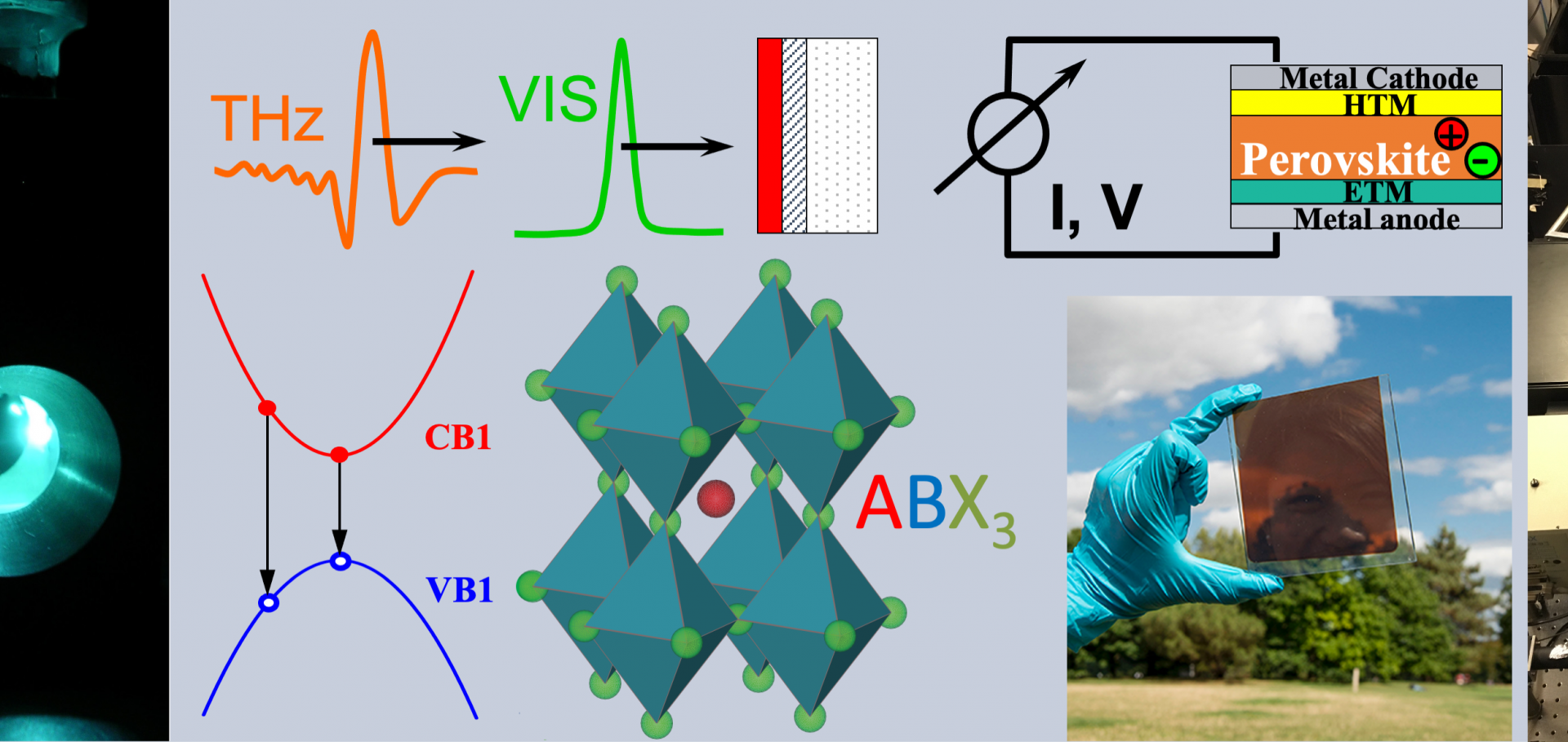
A novel class of semiconducting compounds, metal‐halide perovskites (MHPs), has emerged as a versatile platform for advanced optoelectronic device architectures, offering a unique combination of exceptional physical properties and facile processing. In this study, we present a monolithic high‐speed photodetector capable of directly sensing the time delay between two light pulses with a temporal resolution of at least 170 ps, corresponding to a light propagation distance of ~5 cm—making it well suited for Light Detection and Ranging (LiDAR) applications. This outstanding time resolution is achieved through a signal‐balancing detection scheme that effectively overcomes the limitations of conventional photodetectors, whose response speed is inherently limited by charge‐carrier lifetime and transit time. The device exhibits an exceptionally low noise spectral density, comparable to that of state‐of‐the‐art silicon photodiodes. The fully symmetric device stack comprises a crystalline CsPbBr3 absorber layer tens of microns thick, fabricated via a confined melt process. Comprehensive electro‐optical characterization reveals charge‐carrier lifetimes and mobilities on both microscopic and macroscopic length scales, using transient photoluminescence, time‐resolved photocurrent, time of flight, and terahertz pump–probe spectroscopy. The CsPbBr3 layer exhibits charge‐carrier lifetimes exceeding 100 ns, a microscopic electron–hole mobility of 15 ± 1 cm2 V−1 s−1, and a macroscopic non‐dispersive hole mobility of 8.5 cm2 V−1 s−1. imageCross-polarized and stable second harmonic generation from monocrystalline copper
Nanophotonics De Gruyter 14:25 (2025) 4575-4582
Abstract:
Second-harmonic generation (SHG) is a powerful surface-specific probe for centrosymmetric materials, with broad relevance to energy and biological interfaces. Plasmonic nanomaterials have been extensively utilized to amplify this nonlinear response. Yet, material instability has constrained most studies to gold, despite the significance of plasmonic metals such as copper for catalysis. Here, we demonstrate stable and anisotropic SHG from monocrystalline copper, overcoming long-standing challenges associated with surface degradation. By leveraging an on-substrate synthesis approach that yields atomically flat and oxidation-resistant Cu microflakes, we enable reliable SHG measurements and reveal a strong cross-polarized response with C 3v surface symmetry. The SHG signal remains stable over 3 h of continuous femtosecond excitation, highlighting the remarkable optical robustness of the Cu microflakes. These results reinforce the viability of monocrystalline Cu as a robust platform for nonlinear nanophotonics and surface-sensitive spectroscopy, expanding the range of copper-based optical applications.Correlated Vibrational and Electronic Signatures of Surface Disorder in CsPbBr 3 Nanocrystals
ACS Nano American Chemical Society 19:46 (2025) 40159-40169