Topological Dirac semi-metals as novel, optically-switchable, helicity-dependent terahertz sources
2022 47th International Conference on Infrared, Millimeter and Terahertz Waves (IRMMW-THz) IEEE (2022)
Abstract:
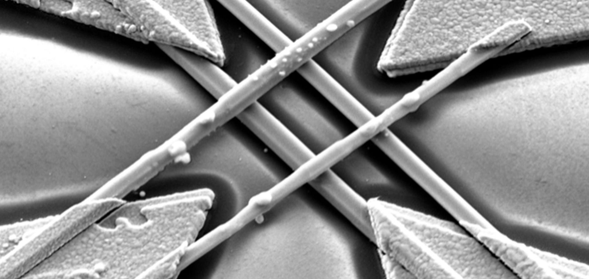
The generation and control of terahertz pulses is vital for realizing the potential of terahertz radiation in several sectors, including 6G communication, security and imaging. In this work, we present the topological Dirac semimetal cadmium arsenide as a novel helicity-dependent terahertz source. We show both broadband (single-cycle) and narrowband (multi-cycle) terahertz pulses upon near-infrared photoexcitation at oblique incidence. By varying the incident angle of the photoexcitation pulse, control of the emission frequency can also be achieved, providing a candidate for a tuneable narrowband terahertz source.Polarization anisotropy in nanowires: Fundamental concepts and progress towards terahertz-band polarization devices
Progress in Quantum Electronics Elsevier 85 (2022) 100417
Abstract:
Pronounced polarization anisotropy in semiconductor nanowires has been exploited to achieve polarization-sensitive devices operating across the electromagnetic spectrum, from the ultraviolet to the terahertz band. This contribution describes the physical origins of optical and electrical anisotropy in nanowires. Polarization anisotropy arising from dielectric contrast, and the behaviour of (nano)wire grid polarizers, are derived from first principles. This review discusses experimental observations of polarization-sensitive light–matter interactions in nanowires. It then describes how these phenomena are employed in devices that detect or modulate polarized terahertz radiation on ultrafast timescales. Such novel terahertz device concepts are expected to find use in a wide variety of applications including high-speed terahertz-band communications and molecular fingerprinting.Impact of hole-transport layer and interface passivation on halide segregation in mixed-halide perovskites
Advanced Functional Materials Wiley 32:41 (2022) 2204825
Abstract:
Mixed-halide perovskites offer ideal bandgaps for tandem solar cells, but photoinduced halide segregation compromises photovoltaic device performance. This study explores the influence of a hole-transport layer, necessary for a full device, by monitoring halide segregation through in situ, concurrent X-ray diffraction and photoluminescence measurements to disentangle compositional and optoelectronic changes. This work demonstrates that top coating FA0.83Cs0.17Pb(Br0.4I0.6)3 perovskite films with a poly(triaryl)amine (PTAA) hole-extraction layer surprisingly leads to suppression of halide segregation because photogenerated charge carriers are rapidly trapped at interfacial defects that do not drive halide segregation. However, the generation of iodide-enriched regions near the perovskite/PTAA interface enhances hole back-transfer from the PTAA layer through improved energy level offsets, increasing radiative recombination losses. It is further found that while passivation with a piperidinium salt slows halide segregation in perovskite films, the addition of a PTAA top-coating accelerates such effects, elucidating the specific nature of trap types that are able to drive the halide segregation process. This work highlights the importance of selective passivation techniques for achieving efficient and stable wide-bandgap perovskite photovoltaic devices.Applicability of tin-iodide perovskites for hot-carrier PV devices – ultrafast pump-push-probe study of hot-carrier cooling dynamics
Fundacio Scito (2022)
Visualizing macroscopic inhomogeneities in perovskite solar cells
ACS Energy Letters American Chemical Society 7:7 (2022) 2311-2322