Control Over the Microstructure of Vapor‐Deposited CsPbBr 3 Enhances Amplified Spontaneous Emission
Advanced Optical Materials Wiley (2025) e02160
Abstract:
Inorganic cesium‐based metal halide perovskite (MHP) semiconductors have great potential as active layers in optoelectronic devices, such as perovskite light‐emitting diodes (PeLEDs) and perovskite lasers. However, precise control of crystal type, quality, and thickness is required to create high‐performance and reproducible devices. Vapor‐phase vacuum deposition enables fabrication of MHP thin films and devices with excellent uniformity and control over layer thickness, although a full understanding of crystal growth mechanisms and products has proved elusive. Here, conditions of vapor co‐deposition of CsBr and PbBr are related with the optical performance and atomic microstructure of resulting CsPbBr3 thin films. It is found that the structure is predominantly photoactive γ‐CsPbBr3 over a wide range of conditions, but the presence of impurity phases and Ruddlesden–Popper (RP) planar defects both degrade optical performance as quantified through measured amplified spontaneous emission (ASE) thresholds. Furthermore, the atomic structure of the dominant impurity phases is resolved: CsPb2Br5 and Cs4PbBr6. It is revealed that a small nominal excess of CsBr‐precursor flux during co‐evaporation can significantly enhance the nucleation of thin films, resulting in well‐defined grains greater than 500 nm in size and the relative suppression of RP planar defects. Such films exhibit intensified photoluminescence (PL) emission and a reduced ASE threshold of 30.9 µJ cm−2.Optically Determined Hole Effective Mass in Tin-Iodide Perovskite Films
ACS Energy Letters American Chemical Society 10:9 (2025) 4589-4595
Abstract:
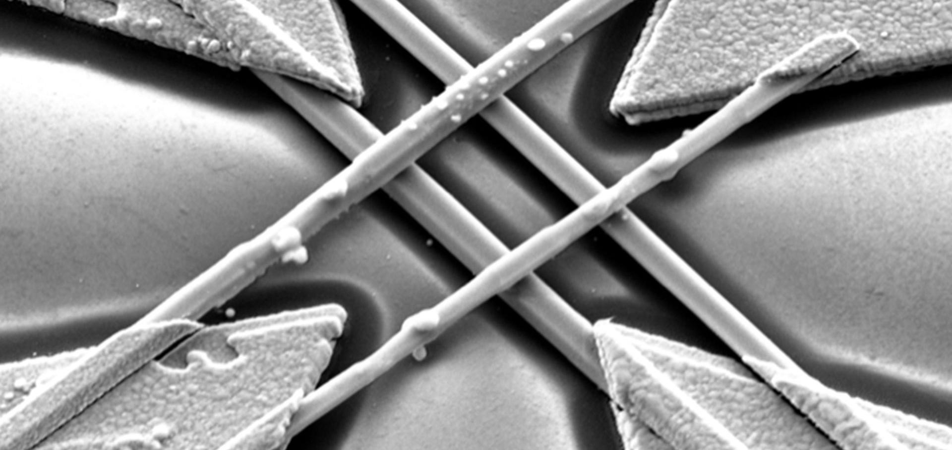
Tin-halide perovskites currently offer the best photovoltaic performance of lead-free metal-halide semiconductors. However, their transport properties are mostly dominated by holes, owing to ubiquitous self-doping. Here we demonstrate a noncontact, optical spectroscopic method to determine the effective mass of the dominant hole species in FASnI3, by investigating a series of thin films with hole densities finely tuned through either SnF2 additive concentration or controlled exposure to air. We accurately determine the plasma frequency from mid-infrared reflectance spectra by modeling changes in the vibrational response of the FA cation as the plasma edge shifts through the molecular resonance. Our approach yields a hole effective mass of 0.28m e for FASnI3 and demonstrates parabolicity within ∼100 meV of the valence band edge. An absence of Fano contributions further highlights insignificant coupling between the hole plasma and FA cation. Overall, this approach enables noncontact screening of thin-film materials for optimized charge-carrier transport properties.Probing of Terahertz Conductivity in Single InAs Nanowire with Resonance-Amplified Near-Field Spectroscopy
Institute of Electrical and Electronics Engineers (IEEE) 00 (2025) 1-2
Abstract:
We present a terahertz (THz) resonance-amplified near-field spectroscopy technique for detecting subtle changes in THz conductivity of an isolated nanoscale system – single InAs nanowire – under ultrafast photoexcitation. Using spatial field localisation and resonant enhancement in a bowtie antenna gap, we quantitatively characterise conductivity variations due to the addition of ~200 electrons via changes in the antenna’s resonance, unlocking studies of ultrafast charge carrier dynamics in isolated nanoscale systems.Carrier-Envelope Phase Control in Terahertz Pulse Generation Using InAs Ribbon Metasurfaces
ACS Photonics American Chemical Society 12:8 (2025) 4534-4539
Abstract:
Generation of broadband terahertz (THz) pulses with variable polarization and carrier-envelope phase can enable the tailoring of THz beam wavefronts for advanced applications in THz imaging and spectroscopy and for strong THz field optics. While metasurfaces composed of deeply subwavelength THz emitters have recently been demonstrated to define the polarization and spatial profile of the generated THz fields, precise phase control or synthesis of THz pulse waveforms remains a challenging problem. Here, we propose and demonstrate metasurfaces composed of indium arsenide (InAs) nanoscale ribbon arrays capable of generating THz pulses with variable carrier-envelope phase. We show that different THz generation mechanisms, each contributing distinct phases, can be activated in the ribbons, enabling carrier-envelope phase control spanning a range of π over a wide band of frequencies (∼1-3 THz). This is achieved solely through the ribbon array geometry using linearly polarized optical excitation of the ribbons. The arrays enable precise control of the THz phase and amplitude, opening the door to advanced structured THz wavefront synthesis using ultrathin dielectric metasurfaces.Impact of Charge Transport Layers on the Structural and Optoelectronic Properties of Coevaporated Cu 2 AgBiI 6
ACS Applied Materials & Interfaces American Chemical Society 17:28 (2025) 40363-40374