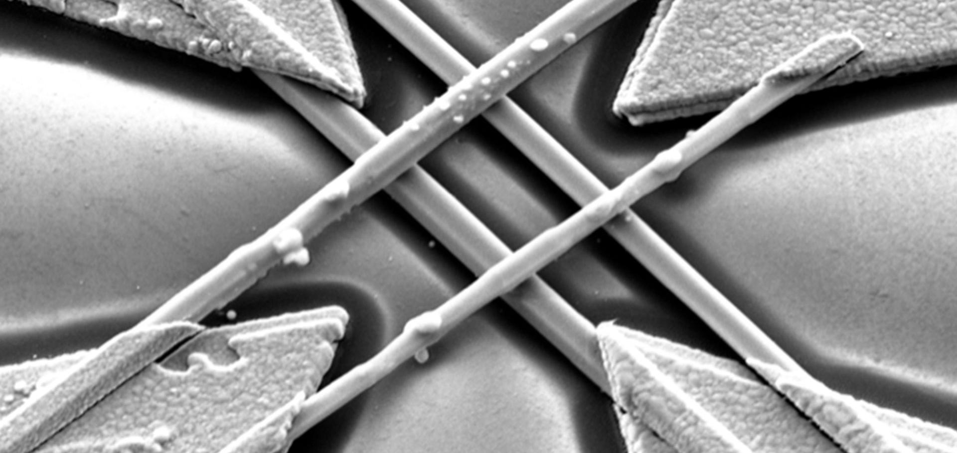
A thorough experimental assessment of THz-TDS plasma diagnostic techniques for nuclear fusion applications
Alumina nanoparticles enable optimal spray-coated perovskite thin film growth on self-assembled monolayers for efficient and reproducible photovoltaics
Contrasting Ultra-Low Frequency Raman and Infrared Modes in Emerging Metal Halides for Photovoltaics
Abstract:
Lattice dynamics are critical to photovoltaic material performance, governing dynamic disorder, hot-carrier cooling, charge-carrier recombination, and transport. Soft metal-halide perovskites exhibit particularly intriguing dynamics, with Raman spectra exhibiting an unusually broad low-frequency response whose origin is still much debated. Here, we utilize ultra-low frequency Raman and infrared terahertz time-domain spectroscopies to provide a systematic examination of the vibrational response for a wide range of metal-halide semiconductors: FAPbI3, MAPbI x Br3–x , CsPbBr3, PbI2, Cs2AgBiBr6, Cu2AgBiI6, and AgI. We rule out extrinsic defects, octahedral tilting, cation lone pairs, and “liquid-like” Boson peaks as causes of the debated central Raman peak. Instead, we propose that the central Raman response results from an interplay of the significant broadening of Raman-active, low-energy phonon modes that are strongly amplified by a population component from Bose–Einstein statistics toward low frequency. These findings elucidate the complexities of light interactions with low-energy lattice vibrations in soft metal-halide semiconductors emerging for photovoltaic applications.In situ nanoscopy of single-grain nanomorphology and ultrafast carrier dynamics in metal halide perovskites
In situ nanoscopy of single-grain nanomorphology and ultrafast carrier dynamics in metal halide perovskites
Abstract:
Designing next-generation light-harvesting devices requires a detailed understanding of the transport of photoexcited charge carriers. The record-breaking efficiencies of metal halide perovskite solar cells have been linked to effective charge-carrier diffusion, yet the exact nature of charge-carrier out-of-plane transport remains notoriously difficult to explain. The characteristic spatial inhomogeneity of perovskite films with nanograins and crystallographic disorder calls for the simultaneous and hitherto elusive in situ resolution of the chemical composition, the structural phase and the ultrafast dynamics of the local out-of-plane transport. Here we simultaneously probe the intrinsic out-of-plane charge-carrier diffusion and the nanoscale morphology by pushing depth-sensitive terahertz near-field nanospectroscopy to extreme subcycle timescales. In films of the organic–inorganic metal halide perovskite FA0.83Cs0.17Pb(I1−xClx)3 (where FA is formamidinium), domains of the cubic α-phase are clearly distinguished from the trigonal δ-phase and PbI2 nano-islands. By analysing deep-subcycle time shifts of the scattered terahertz waveform after photoexcitation, we access the vertical charge-carrier dynamics within single grains. At all of the measured locations, despite topographic irregularities, diffusion is surprisingly homogeneous on the 100 nm scale, although it varies between mesoscopic regions. Linking in situ carrier transport with nanoscale morphology and chemical composition could introduce a paradigm shift for the analysis and optimization of next-generation optoelectronics that are based on nanocrystalline materials.