Optoelectronics: Fast silicon photodiodes
Nature Photonics Nature Publishing Group 11:5 (2017) 268-269
Abstract:
How much internet traffic did you generate today? Perhaps more than you realise given the increasing popularity of streaming audio or video content, “cloud” data storage, and social media. It is estimated that approximately 1 zettabyte (1021 bytes) of internet traffic was transmitted globally last year,1 which is the equivalent of about 360MB per day per person in the world. Much of the long distance, high volume internet traffic is transmitted via near infrared (NIR) light through optical fibre waveguides. At the end of the optical fibre the optical signal is turned into an electrical signal, typically for use in silicon based integrated circuits. However, presently most receivers for long distance optical fibre communications systems are based on photodiodes made from other semiconductors such as InxGa1-xAs, or Ge which are challenging and costly to integrate with silicon CMOS electronics on a single chip.The influence of surfaces on the transient terahertz conductivity and electron mobility of GaAs nanowires
Journal of Physics D: Applied Physics IOP Publishing 50:22 (2017) 224001
Abstract:
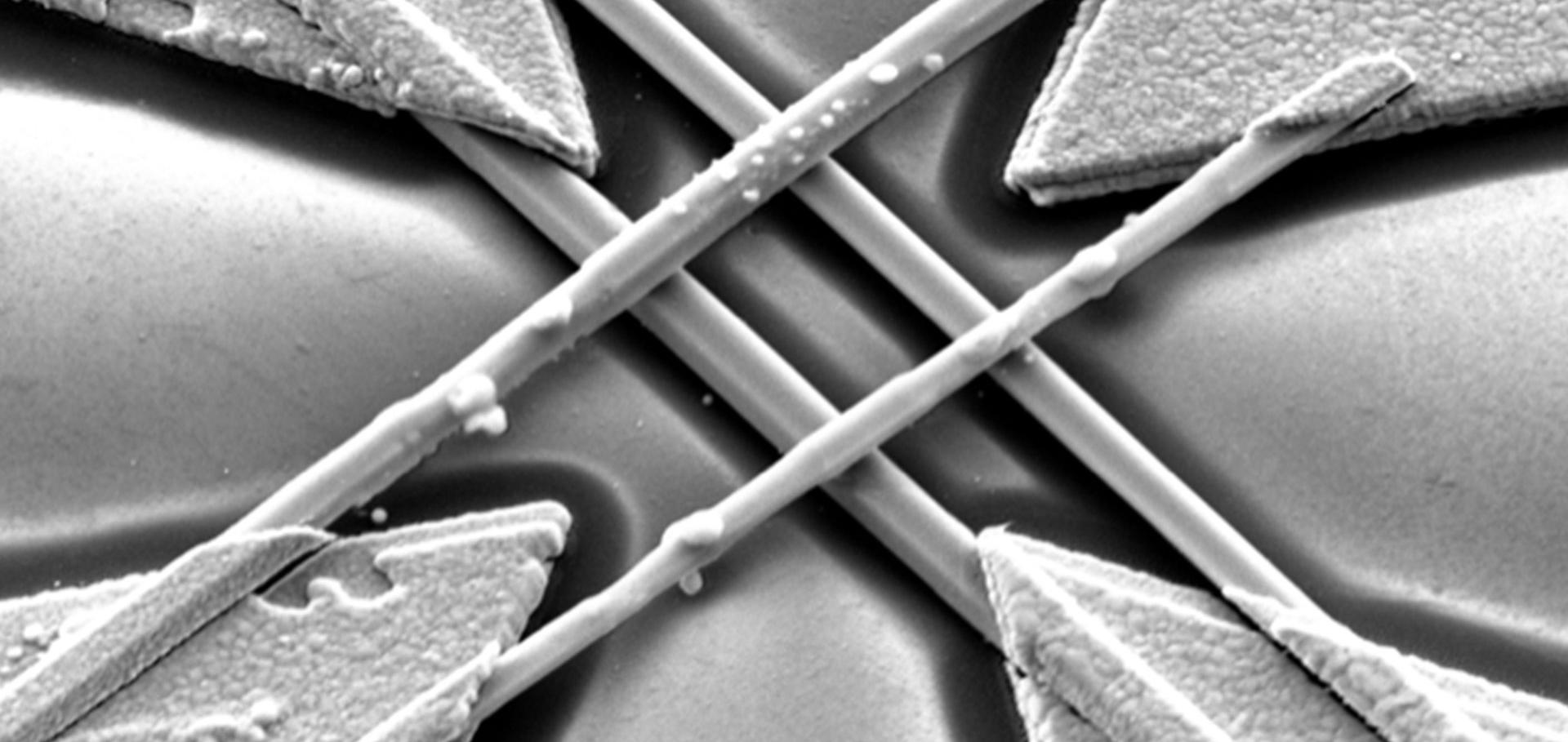
Bare unpassivated GaAs nanowires feature relatively high electron mobilities (400–2100 cm2 V−1 s−1) and ultrashort charge carrier lifetimes (1–5 ps) at room temperature. These two properties are highly desirable for high speed optoelectronic devices, including photoreceivers, modulators and switches operating at microwave and terahertz frequencies. When engineering these GaAs nanowire-based devices, it is important to have a quantitative understanding of how the charge carrier mobility and lifetime can be tuned. Here we use optical-pump–terahertz-probe spectroscopy to quantify how mobility and lifetime depend on the nanowire surfaces and on carrier density in unpassivated GaAs nanowires. We also present two alternative frameworks for the analysis of nanowire photoconductivity: one based on plasmon resonance and the other based on Maxwell–Garnett effective medium theory with the nanowires modelled as prolate ellipsoids. We find the electron mobility decreases significantly with decreasing nanowire diameter, as charge carriers experience increased scattering at nanowire surfaces. Reducing the diameter from 50 nm to 30 nm degrades the electron mobility by up to 47%. Photoconductivity dynamics were dominated by trapping at saturable states existing at the nanowire surface, and the trapping rate was highest for the nanowires of narrowest diameter. The maximum surface recombination velocity, which occurs in the limit of all traps being empty, was calculated as 1.3 × 106 cm s−1. We note that when selecting the optimum nanowire diameter for an ultrafast device, there is a trade-off between achieving a short lifetime and a high carrier mobility. To achieve high speed GaAs nanowire devices featuring the highest charge carrier mobilities and shortest lifetimes, we recommend operating the devices at low charge carrier densities.Single n+-i-n+ InP Nanowires for Highly Sensitive Terahertz Detection
Nanotechnology IOP Publishing Ltd 28 (2017) 125202
Abstract:
Developing single-nanowire terahertz (THz) electronics and employing them as sub-wavelength components for highly-integrated THz time-domain spectroscopy (THz-TDS) applications are a promising approach to achieve future low-cost, highly integrable and high-resolution THz tools, which are desirable in many areas spanning from security, industry, environmental monitoring and medical diagnostics to fundamental science. In this work, we present the design and growth of n+-i-n+ InP nanowires. The axial doping profile of the n+-i-n+ InP nanowires has been calibrated and characterized using combined optical and electrical approaches to achieve nanowire devices with low contact resistances, on which the highly-sensitive InP single-nanowire photoconductive THz detectors have been demonstrated. While the n+-i-n+ InP nanowire detector has a only pA-level response current, it has a 2.5 times improved signal-to-noise ratio compared with the undoped InP nanowire detector and is comparable to traditional bulk THz detectors. This performance indicates a promising path to nanowire-based THz electronics for future commercial applications.The 2017 terahertz science and technology roadmap
Journal of Physics D: Applied Physics IOP Publishing 50:4 (2017)
Abstract:
Science and technologies based on terahertz frequency electromagnetic radiation (100 GHz-30 THz) have developed rapidly over the last 30 years. For most of the 20th Century, terahertz radiation, then referred to as sub-millimeter wave or far-infrared radiation, was mainly utilized by astronomers and some spectroscopists. Following the development of laser based terahertz time-domain spectroscopy in the 1980s and 1990s the field of THz science and technology expanded rapidly, to the extent that it now touches many areas from fundamental science to 'real world' applications. For example THz radiation is being used to optimize materials for new solar cells, and may also be a key technology for the next generation of airport security scanners. While the field was emerging it was possible to keep track of all new developments, however now the field has grown so much that it is increasingly difficult to follow the diverse range of new discoveries and applications that are appearing. At this point in time, when the field of THz science and technology is moving from an emerging to a more established and interdisciplinary field, it is apt to present a roadmap to help identify the breadth and future directions of the field. The aim of this roadmap is to present a snapshot of the present state of THz science and technology in 2017, and provide an opinion on the challenges and opportunities that the future holds. To be able to achieve this aim, we have invited a group of international experts to write 18 sections that cover most of the key areas of THz science and technology. We hope that The 2017 Roadmap on THz science and technology will prove to be a useful resource by providing a wide ranging introduction to the capabilities of THz radiation for those outside or just entering the field as well as providing perspective and breadth for those who are well established. We also feel that this review should serve as a useful guide for government and funding agencies.Cs2InAgCl6: A new lead-free halide double perovskite with direct band gap.
Journal of Physical Chemistry Letters American Chemical Society 2017:8 (2017) 772-778