Perovskite-perovskite tandem photovoltaics with optimized bandgaps
Science American Association for the Advancement of Science (2016)
Abstract:
Multi-junction solar photovoltaics are proven to deliver the highest performance of any solar cell architecture, making them ideally suited for deployment in an increasingly efficiency driven solar industry. Conventional multi-junction cells reach up to 45% efficiency, but are so costly to manufacture that they are only currently useful for space and solar concentrator photovoltaics. Here, we demonstrate the first four and two-terminal perovskite-perovskite tandem solar cells with ideally matched bandgaps. We develop an infrared absorbing 1.2eV bandgap perovskite, FA0.75Cs0.25Sn0.5Pb0.5I3, which is capable of delivering 13.6% efficiency. By combining this material with a wider bandgap FA0.83Cs0.17Pb(I0.5Br0.5)3 material, we reach initial monolithic two terminal tandem efficiencies of 14.0 % with over 1.75 V open circuitvoltage. We also make mechanically stacked four terminal tandem cells and obtain 18.1 % efficiency for small cells, and 16.0 % efficiency for 1cm^2 cells. Crucially, we find that our infrared absorbing perovskite cells exhibit excellent thermal and atmospheric stability, unprecedented for Sn based perovskites. This device architecture and materials set will enable “all perovskite” thin film solar cells to reach the highest efficiencies in the long term at the lowest costs, delivering a viable photovoltaic technology to supplant fossil fuels.Radiative Monomolecular Recombination Boosts Amplified Spontaneous Emission in HC(NH2)2SnI3 Perovskite Films.
Journal of Physical Chemistry Letters American Chemical Society 7:20 (2016) 4178-4184
Abstract:
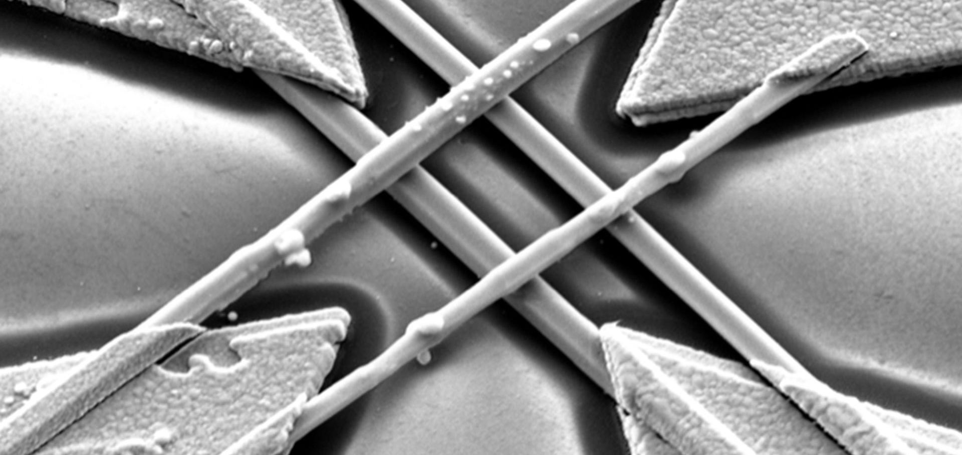
Hybrid metal-halide perovskites have potential as cost-effective gain media for laser technology because of their superior optoelectronic properties. Although lead-halide perovskites have been most widely studied to date, tin-based perovskites have been proposed as a less toxic alternative. In this Letter, we show that amplified spontaneous emission (ASE) in formamidinium tin triiodide (FASnI3) thin films is supported by an observed radiative monomolecular charge recombination pathway deriving from its unintentional doping. Such a radiative component will be active even at the lowest charge-carrier densities, opening a pathway for ultralow light-emission thresholds. Using time-resolved THz photoconductivity analysis, we further show that the material has an unprecedentedly high charge-carrier mobility of 22 cm(2) V(-1) s(-1) favoring efficient transport. In addition, FASnI3 exhibits strong radiative bimolecular recombination and Auger rates that are over an order of magnitude lower than for lead-halide perovskites. In combination, these properties reveal that tin-halide perovskites are highly suited to light-emitting devices.Efficiency enhancement of axial junction InP single nanowire solar cells by dielectric coating
Nano Energy Elsevier 28 (2016) 106-114
Charge-carrier dynamics in 2D hybrid metal-halide perovskites
Nano letters American Chemical Society 16:11 (2016) 7001-7007
Abstract:
Hybrid metal halide perovskites are promising new materials for use in solar cells, however, their chemical stability in the presence of moisture remains a significant drawback. Quasi two-dimensional perovskites that incorporate hydrophobic organic interlayers offer improved resistance to degradation by moisture, currently still at the cost of overall cell efficiency. To elucidate the factors affecting the optoelectronic properties of these materials, we have investigated the charge transport properties and crystallographic orientation of mixed methylammonium (MA)/phenylethylammonium (PEA) lead iodide thin films as a function of MA:PEA and thus the thickness of the 'encapsulated' MA lead halide layers. We find that monomolecular charge-carrier recombination rates first decrease with increasing PEA fraction, most likely as a result of trap passivation, but then increase significantly as excitonic effects begin to dominate for thin confined layers. Bimolecular and Auger recombination rate constants are found to be sensitive to changes in electronic confinement, which alters the density of states for electronic transitions. We demonstrate that effective charge-carrier mobilities remain remarkably high (near 10 cm2/Vs) for intermediate PEA content and are enhanced for preferential orientation of the conducting lead-iodide layers along the probing electric field. The tradeoff between trap reduction, electronic confinement and layer orientation leads to calculated charge-carrier diffusion lengths reaching a maximum of 2.5 µm for intermediate PEA content (50%).A low viscosity, low boiling point, clean solvent system for the rapid crystallisation of highly specular perovskite films
Energy and Environmental Science Royal Society of Chemistry 10:1 (2016) 145-152