
Overcoming Charge-Carrier Localisation in Metal Chalcohalides
Fundacio Scito (2025)
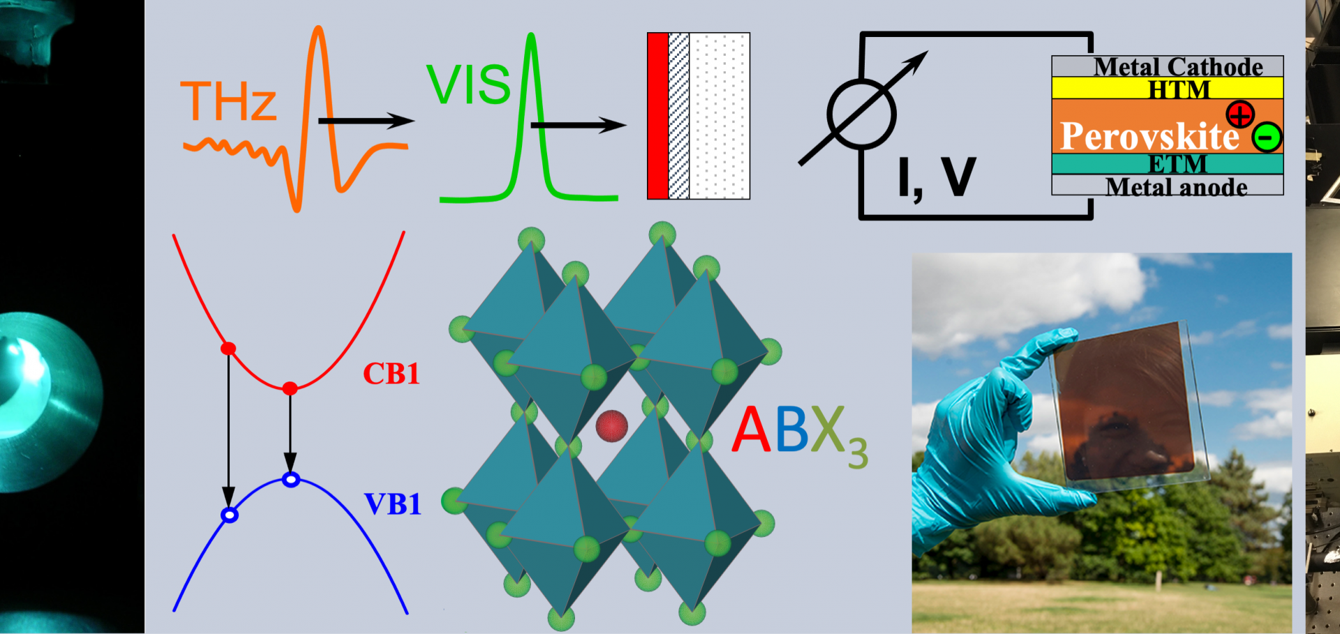
Perovskite‐based time‐domain signal‐balancing LiDAR sensor with centimeter depth resolution
InfoMat Wiley (2025) e70104
Abstract:
A novel class of semiconducting compounds, metal‐halide perovskites (MHPs), has emerged as a versatile platform for advanced optoelectronic device architectures, offering a unique combination of exceptional physical properties and facile processing. In this study, we present a monolithic high‐speed photodetector capable of directly sensing the time delay between two light pulses with a temporal resolution of at least 170 ps, corresponding to a light propagation distance of ~5 cm—making it well suited for Light Detection and Ranging (LiDAR) applications. This outstanding time resolution is achieved through a signal‐balancing detection scheme that effectively overcomes the limitations of conventional photodetectors, whose response speed is inherently limited by charge‐carrier lifetime and transit time. The device exhibits an exceptionally low noise spectral density, comparable to that of state‐of‐the‐art silicon photodiodes. The fully symmetric device stack comprises a crystalline CsPbBr3 absorber layer tens of microns thick, fabricated via a confined melt process. Comprehensive electro‐optical characterization reveals charge‐carrier lifetimes and mobilities on both microscopic and macroscopic length scales, using transient photoluminescence, time‐resolved photocurrent, time of flight, and terahertz pump–probe spectroscopy. The CsPbBr3 layer exhibits charge‐carrier lifetimes exceeding 100 ns, a microscopic electron–hole mobility of 15 ± 1 cm2 V−1 s−1, and a macroscopic non‐dispersive hole mobility of 8.5 cm2 V−1 s−1. imageCorrelated Vibrational and Electronic Signatures of Surface Disorder in CsPbBr 3 Nanocrystals
ACS Nano American Chemical Society 19:46 (2025) 40159-40169
Abstract:
Lead halide perovskite nanocrystals have emerged as promising candidates for classical light-emitting devices and single-photon sources, owing to their high photoluminescence quantum yield, narrow emission line width and tunable emission. Judicious choice of ligands to passivate nanocrystal surfaces has proven to be critical to the structural stability and optoelectronic performance of such nanocrystals. While many ligands have been deployed, the resulting quality of the nanocrystal surface can be difficult to assess directly. Here, we demonstrate ultralow frequency Raman spectroscopy as a powerful tool to resolve surface-sensitive changes in size and ligand choice in perovskite nanocrystals. By investigating a size series of CsPbBr3 nanocrystals from the strong (5 nm) to the weak (28 nm) confinement range, we show that the line width of Raman-active modes provides a highly selective metric for surface disorder and quality. We further examine a series of 28 nm diameter nanocrystals with four different zwitterionic ligands, unravelling clear links between varying steric effects and surface quality evident from Raman analysis. Photoluminescence and THz photoconductivity probes reveal an evident correlation of charge-carrier dynamics and radiative emission yields with ligand chemistry and surface quality inferred from phonon broadening. We further show that surface defects preferentially trap hot charge carriers, which affects exciton stability and radiative emission yields. Overall, our approach offers powerful insights into optimizing nanocrystal-ligand boundaries to enhance the performance of nanoscale quantum light sources and optoelectronic devices.Photoactive Thiophene‐Enriched Tetrathienonaphthalene‐Based Covalent Organic Frameworks
Small Wiley (2025) e11000
Abstract:
The optoelectronic properties of covalent organic frameworks (COFs) can be controlled by the design of their molecular building blocks and assembly. Here, a facile and efficient synthetic route is reported for the novel thiophene‐enriched tetrathienonaphthalene (TTN)‐based node 4,4′,4″,4′″‐(naphtho[1,2‐b:4,3‐b′:5,6‐b″:8,7‐b″′]tetrathiophene‐2,5,8,11‐tetrayl)tetraaniline (TTNTA) for constructing imine‐linked COFs. Utilizing TTNTA, highly crystalline, thiophene‐enriched donor–donor (D–D) and donor–acceptor (D–A) COFs, denoted as TT COF and BDT(BT)2 COF, are synthesized using two distinct aldehyde‐functionalized linear linkers: [2,2′‐bithiophene]‐5,5′‐dicarbaldehyde (TT) and 7,7′‐(4,8‐diethoxybenzo[1,2‐b:4,5‐b′]dithiophene‐2,6‐diyl)bis(benzo[c][1,2,5]thiadiazole‐4‐carbaldehyde) (BDT(BT)2), respectively. Highly crystalline and oriented TTNTA COF films on various substrates via a solvothermal method enabled further comprehensive optical and electronic characterizations. Optical‐pump terahertz‐probe spectroscopy revealed effective charge‐carrier mobility values φμ = 0.34 ± 0.04 and 0.18 ± 0.02 cm2V−1s−1 for TT and BDT(BT)2 COF films, respectively. These results reveal distinct charge‐transport characteristics and provide mechanistic insights into their ultrafast charge‐carrier dynamics. The COFs are demonstrated to be photoactive, showing promising potential as photocathodes without co‐catalysts in photoelectrochemical water splitting, with notable photocurrent densities of 10 and 15.3 µA cm−2 after 1 h illumination, respectively. This work highlights the potential of TTNTA‐based COFs in optoelectronic applications and provides insights into the design of thiophene‐enriched COFs with high crystallinity and photoactive behavior.Impact of Halide Alloying on the Phase Segregation of Mixed‐Halide Perovskites
Small Structures Wiley (2025) e202500545