
Disentangling the Effects of Structure and Lone-Pair Electrons in the Lattice Dynamics of Halide Perovskites
(2023)
Topological materials as promising candidates for tuneable helicity-dependent terahertz emitters
Proceedings of SPIE: Terahertz Emitters, Receivers, and Applications XIV Society of Photo-optical Instrumentation Engineers 12683 (2023)
Abstract:
Topological materials have rapidly gained interest as contenders for development of coherent, controllable terahertz emitters. Possessing Weyl nodes either at the surface or within the bulk, they host spin-polarised, helicity-dependent currents that offer possibility to control the emitted THz pulse by changing the polarization of the optical pulses generating the radiation. Here, we show that upon near-infrared excitation at oblique incidence, multi-cycle pulses are generated with a narrow bandwidth of ∼0.4 THz for cadmium arsenide bulk crystals and nanowire ensembles. Both the bandwidth and peak emission frequency of the generated THz radiation can be tuned by respectively varying the photon helicity and angle of incidence of the photoexcitation light.A templating approach to controlling the growth of coevaporated halide perovskites
ACS Energy Letters American Chemical Society 8:10 (2023) 4008-4015
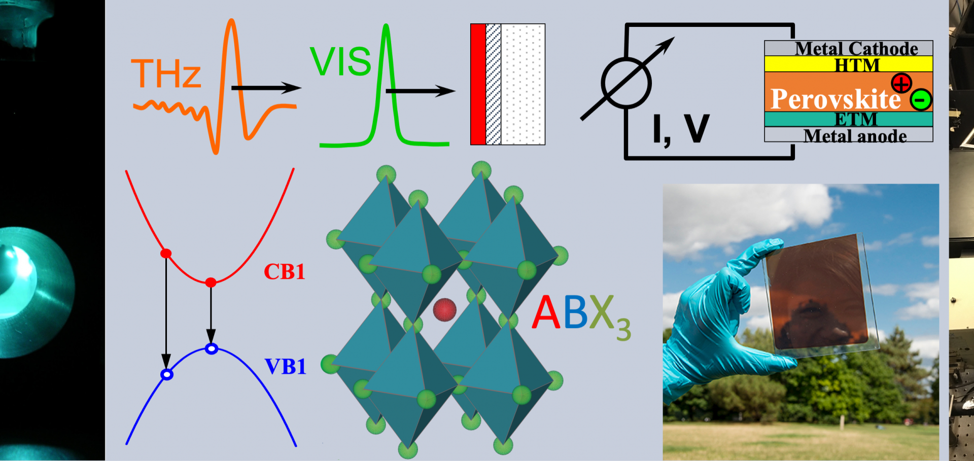
Abstract:
Metal halide perovskite semiconductors have shown significant potential for use in photovoltaic (PV) devices. While fabrication of perovskite thin films can be achieved through a variety of techniques, thermal vapor deposition is particularly promising, allowing for high-throughput fabrication. However, the ability to control the nucleation and growth of these materials, particularly at the charge-transport layer/perovskite interface, is critical to unlocking the full potential of vapor-deposited perovskite PV. In this study, we explore the use of a templating layer to control the growth of coevaporated perovskite films and find that such templating leads to highly oriented films with identical morphology, crystal structure, and optoelectronic properties independent of the underlying layers. Solar cells incorporating templated FA0.9Cs0.1PbI3–xClx show marked improvements with steady-state power conversion efficiency over 19.8%. Our findings provide a straightforward and reproducible method of controlling the charge-transport layer/coevaporated perovskite interface, further clearing the path toward large-scale fabrication of efficient PV devices.Contrasting charge-carrier dynamics across key metal-halide perovskite compositions through in situ simultaneous probes
Advanced Functional Materials Wiley 33:51 (2023) 2305283
Abstract:
Metal-halide perovskites have proven to be a versatile group of semiconductors for optoelectronic applications, with ease of bandgap tuning and stability improvements enabled by halide and cation mixing. However, such compositional variations can be accompanied by significant changes in their charge-carrier transport and recombination regimes that are still not fully understood. Here, a novel combinatorial technique is presented to disentangle such dynamic processes over a wide range of temperatures, based on transient free-space, high-frequency microwave conductivity and photoluminescence measurements conducted simultaneously in situ. Such measurements are used to reveal and contrast the dominant charge-carrier recombination pathways for a range of key compositions: prototypical methylammonium lead iodide perovskite (MAPbI3), the stable mixed formamidinium-caesium lead-halide perovskite FA0.83Cs0.17PbBr0.6I2.4 targeted for photovoltaic tandems with silicon, and fully inorganic wide-bandgap CsPbBr3 aimed toward light sources and X-ray detector applications. The changes in charge-carrier dynamics in FA0.83Cs0.17PbBr0.6I2.4 across temperatures are shown to be dominated by radiative processes, while those in MAPbI3 are governed by energetic disorder at low temperatures, low-bandgap minority-phase inclusions around the phase transition, and non-radiative processes at room temperature. In contrast, CsPbBr3 exhibits significant charge-carrier trapping at low and high temperatures, highlighting the need for improvement of material processing techniques for wide-bandgap perovskites.Chalcohalide Antiperovskite Thin Films with Visible Light Absorption and High Charge-Carrier Mobility Processed by Solvent-Free and Low-Temperature Methods
Chemistry of Materials American Chemical Society (ACS) 35:16 (2023) 6482-6490