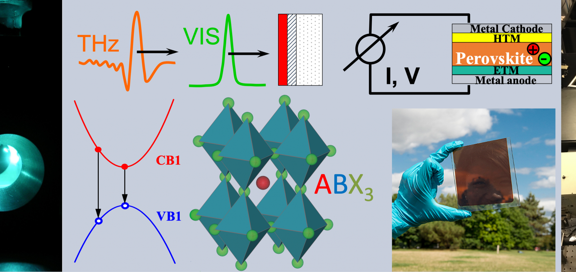
Charge-Carrier Dynamics in Hybrid Metal Halide Perovskites for Photovoltaics and Light Emission
Institute of Electrical and Electronics Engineers (IEEE) (2017) 1-1
Investigations of Doping Via Optical Pump Terahertz-Probe Spectroscopy
Institute of Electrical and Electronics Engineers (IEEE) (2017) 1-1
The entangled triplet pair state in acene and heteroacene materials.
Nature Communications Springer Nature 8 (2017) 15953
Abstract:
Entanglement of states is one of the most surprising and counter-intuitive consequences of quantum mechanics, with potent applications in cryptography and computing. In organic materials, one particularly significant manifestation is the spin-entangled triplet-pair state, which mediates the spin-conserving fission of one spin-0 singlet exciton into two spin-1 triplet excitons. Despite long theoretical and experimental exploration, the nature of the triplet-pair state and inter-triplet interactions have proved elusive. Here we use a range of organic semiconductors that undergo singlet exciton fission to reveal the photophysical properties of entangled triplet-pair states. We find that the triplet pair is bound with respect to free triplets with an energy that is largely material independent (∼30 meV). During its lifetime, the component triplets behave cooperatively as a singlet and emit light through a Herzberg-Teller-type mechanism, resulting in vibronically structured photoluminescence. In photovoltaic blends, charge transfer can occur from the bound triplet pairs with >100% photon-to-charge conversion efficiency.Band-tail recombination in hybrid lead iodide perovskite
Advanced Functional Materials Wiley (2017)
Abstract:
Traps limit the photovoltaic efficiency and affect the charge transport of optoelectronic devices based on hybrid lead halide perovskites. Understanding the nature and energy scale of these trap states is therefore crucial for the development and optimization of solar cell and laser technology based on these materials. Here, the low-temperature photoluminescence of formamidinium lead triiodide (HC(NH2)2PbI3) is investigated. A power-law time dependence in the emission intensity and an additional low-energy emission peak that exhibits an anomalous relative Stokes shift are observed. Using a rate-equation model and a Monte Carlo simulation, it is revealed that both phenomena arise from an exponential trap-density tail with characteristic energy scale of ≈3 meV. Charge-carrier recombination from sites deep within the tail is found to cause emission with energy downshifted by up to several tens of meV. Hence, such phenomena may in part be responsible for open-circuit voltage losses commonly observed in these materials. In this high-quality hybrid perovskite, trap states thus predominantly comprise a continuum of energetic levels (associated with disorder) rather than discrete trap energy levels (associated, e.g., with elemental vacancies). Hybrid perovskites may therefore be viewed as classic semiconductors whose bandstructure picture is moderated by a modest degree of energetic disorder.Crystallization kinetics and morphology control of formamidinium-cesium mixed-cation lead mixed-halide perovskite via tunability of the colloidal precursor solution
Advanced Materials Wiley 29:29 (2017) 1-8


