
Towards higher electron mobility in modulation doped GaAs/AlGaAs core shell nanowires
Nanoscale Royal Society of Chemistry 9 (2017) 7839-7846
Abstract:
Precise control over the electrical conductivity of semiconductor nanowires is a crucial prerequisite for implementation into novel electronic and optoelectronic devices. Advances in our understanding of doping mechanisms in nanowires and their influence on electron mobility and radiative efficiency are urgently required. Here, we investigate the electronic properties of n-type modulation doped GaAs/AlGaAs nanowires via optical pump terahertz (THz) probe spectroscopy and photoluminescence spectroscopy over the temperature range 5K-300K. We directly determine an ionisation energy of 6.7±0.5meV (T = 52K) for the Si donors that create the modulation doping in the AlGaAs shell. We further elucidate the temperature dependence of the electron mobility, photoconductivity lifetime and radiative efficiency, and determine the charge-carrier scattering mechanisms that limit electron mobility. We show that below the donor ionization temperature, charge scattering is limited by interactions with interfaces, leading to an excellent electron mobility of 4360±380cm2V-1s-1 at 5 K. Above the ionization temperature, polar scattering via longitudinal optical (LO) phonons dominates, leading to a room temperature mobility of 2220±130cm2V-1s-1. In addition, we show that the Si donors effectively passivate interfacial trap states in the nanowires, leading to prolonged photoconductivity lifetimes with increasing temperature, accompanied by an enhanced radiative efficiency that exceeds 10% at room temperature.Charge-carrier mobilities in metal halide perovskites: Fundamental mechanisms and limits
ACS Energy Letters American Chemical Society (2017)
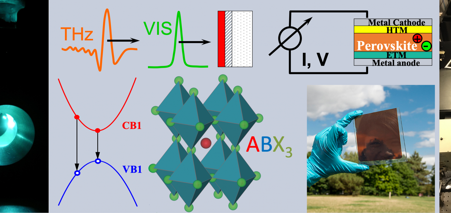
Abstract:
Perovskite photovoltaic cells have seen a remarkable rise in power conversion efficiencies over a period of only a few years. Much of this performance is underpinned by the favorable chargecarrier mobilities in metal halide perovskites (MHPs), which are remarkably high for materials with such facile and versatile processing routes. This Perspective outlines the mechanisms that set a fundamental upper limit to charge-carrier mobility values in MHPs and reveals how they may be tuned through changes in stoichiometry. In addition, extrinsic effects such as grain size, energetic disorder, and self-doping are discussed for specific MHPs in the context of remedies designed to avoid them.The influence of surfaces on the transient terahertz conductivity and electron mobility of GaAs nanowires
Journal of Physics D: Applied Physics IOP Publishing 50:22 (2017) 224001
Abstract:
Bare unpassivated GaAs nanowires feature relatively high electron mobilities (400–2100 cm2 V−1 s−1) and ultrashort charge carrier lifetimes (1–5 ps) at room temperature. These two properties are highly desirable for high speed optoelectronic devices, including photoreceivers, modulators and switches operating at microwave and terahertz frequencies. When engineering these GaAs nanowire-based devices, it is important to have a quantitative understanding of how the charge carrier mobility and lifetime can be tuned. Here we use optical-pump–terahertz-probe spectroscopy to quantify how mobility and lifetime depend on the nanowire surfaces and on carrier density in unpassivated GaAs nanowires. We also present two alternative frameworks for the analysis of nanowire photoconductivity: one based on plasmon resonance and the other based on Maxwell–Garnett effective medium theory with the nanowires modelled as prolate ellipsoids. We find the electron mobility decreases significantly with decreasing nanowire diameter, as charge carriers experience increased scattering at nanowire surfaces. Reducing the diameter from 50 nm to 30 nm degrades the electron mobility by up to 47%. Photoconductivity dynamics were dominated by trapping at saturable states existing at the nanowire surface, and the trapping rate was highest for the nanowires of narrowest diameter. The maximum surface recombination velocity, which occurs in the limit of all traps being empty, was calculated as 1.3 × 106 cm s−1. We note that when selecting the optimum nanowire diameter for an ultrafast device, there is a trade-off between achieving a short lifetime and a high carrier mobility. To achieve high speed GaAs nanowire devices featuring the highest charge carrier mobilities and shortest lifetimes, we recommend operating the devices at low charge carrier densities.Cs2InAgCl6: A new lead-free halide double perovskite with direct band gap.
Journal of Physical Chemistry Letters American Chemical Society 2017:8 (2017) 772-778
Abstract:
A2BB'X6 halide double perovskites based on bismuth and silver have recently been proposed as potential environmentally friendly alternatives to lead-based hybrid halide perovskites. In particular, Cs2BiAgX6 (X = Cl, Br) have been synthesized and found to exhibit band gaps in the visible range. However, the band gaps of these compounds are indirect, which is not ideal for applications in thin film photovoltaics. Here, we propose a new class of halide double perovskites, where the B(3+) and B(+) cations are In(3+) and Ag(+), respectively. Our first-principles calculations indicate that the hypothetical compounds Cs2InAgX6 (X = Cl, Br, I) should exhibit direct band gaps between the visible (I) and the ultraviolet (Cl). Based on these predictions, we attempt to synthesize Cs2InAgCl6 and Cs2InAgBr6, and we succeed to form the hitherto unknown double perovskite Cs2InAgCl6. X-ray diffraction yields a double perovskite structure with space group Fm3̅m. The measured band gap is 3.3 eV, and the compound is found to be photosensitive and turns reversibly from white to orange under ultraviolet illumination. We also perform an empirical analysis of the stability of Cs2InAgX6 and their mixed halides based on Goldschmidt's rules, and we find that it should also be possible to form Cs2InAg(Cl1-xBrx)6 for x < 1. The synthesis of mixed halides will open the way to the development of lead-free double perovskites with direct and tunable band gaps.Semiconductor Nanowires in Terahertz Photonics: From Spectroscopy to Ultrafast Nanowire-Based Devices
Institute of Electrical and Electronics Engineers (IEEE) (2017) 1-2