Electronic correlation and pseudogap-like behavior of high-temperature superconductor La3Ni2O7
Chinese Physics Letters IOP Publishing 41:8 (2024) 087402
Abstract:
High-temperature superconductivity (HTSC) remains one of the most challenging and fascinating mysteries in condensed matter physics. Recently, superconductivity with transition temperature exceeding liquid-nitrogen temperature is discovered in La3Ni2O7 at high pressure, which provides a new platform to explore the unconventional HTSC. In this work, using high-resolution angle-resolved photoemission spectroscopy and ab initio calculation, we systematically investigate the electronic structures of La3Ni2O7 at ambient pressure. Our experiments are in nice agreement with ab initio calculations after considering an orbital-dependent band renormalization effect. The strong electron correlation effect pushes a flat band of dz2 orbital component below the Fermi level (EF), which is predicted to locate right at EF under high pressure. Moreover, the dx2–y2 band shows pseudogap-like behavior with suppressed spectral weight and diminished quasiparticle peak near EF. Our findings provide important insights into the electronic structure of La3Ni2O7, which will shed light on understanding of the unconventional superconductivity in nickelates.Evidence of strong and mode-selective electron–phonon coupling in the topological superconductor candidate 2M-WS 2
Nature Communications Nature Research 15:1 (2024) 6235
Abstract:
The interaction between lattice vibrations and electrons plays a key role in various aspects of condensed matter physics — including electron hydrodynamics, strange metal behavior, and high-temperature superconductivity. In this study, we present systematic investigations using Raman scattering and angle-resolved photoemission spectroscopy (ARPES) to examine the phononic and electronic subsystems of the topological superconductor candidate 2M-WS2. Raman scattering exhibits an anomalous nonmonotonic temperature dependence of phonon linewidths, indicative of strong phonon–electron scattering over phonon–phonon scattering. The ARPES results demonstrate pronounced dispersion anomalies (kinks) at multiple binding energies within both bulk and topological surface states, indicating a robust and mode-selective coupling between the electronic states and various phonon modes. These experimental findings align with previous calculations of the Eliashberg function, providing a deeper understanding of the highest superconducting transition temperature observed in 2M-WS2 (8.8 K) among all transition metal dichalcogenides as induced by electron–phonon coupling. Furthermore, our results may offer valuable insights into other properties of 2M-WS2 and guide the search for high-temperature topological superconductors.Evidence of strong and mode-selective electron–phonon coupling in the topological superconductor candidate 2M-WS2
Nature Communications Springer Nature 15:1 (2024) 6235
Abstract:
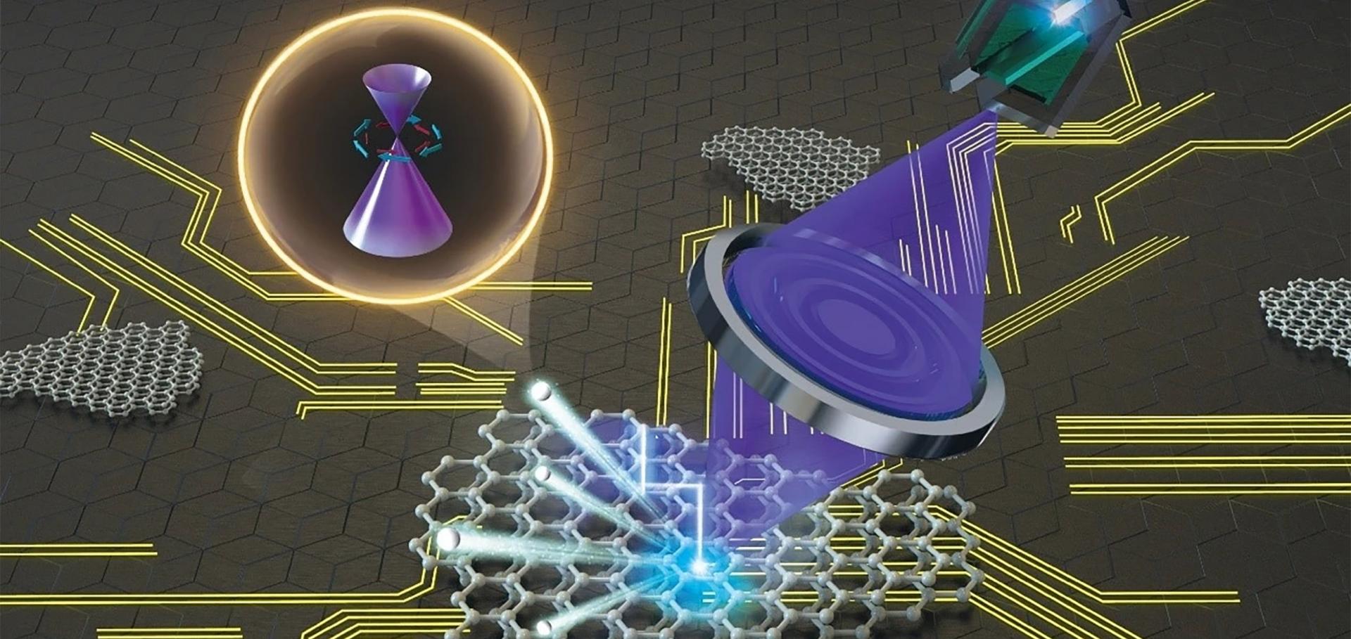
The interaction between lattice vibrations and electrons plays a key role in various aspects of condensed matter physics — including electron hydrodynamics, strange metal behavior, and high-temperature superconductivity. In this study, we present systematic investigations using Raman scattering and angle-resolved photoemission spectroscopy (ARPES) to examine the phononic and electronic subsystems of the topological superconductor candidate 2M-WS2. Raman scattering exhibits an anomalous nonmonotonic temperature dependence of phonon linewidths, indicative of strong phonon–electron scattering over phonon–phonon scattering. The ARPES results demonstrate pronounced dispersion anomalies (kinks) at multiple binding energies within both bulk and topological surface states, indicating a robust and mode-selective coupling between the electronic states and various phonon modes. These experimental findings align with previous calculations of the Eliashberg function, providing a deeper understanding of the highest superconducting transition temperature observed in 2M-WS2 (8.8 K) among all transition metal dichalcogenides as induced by electron–phonon coupling. Furthermore, our results may offer valuable insights into other properties of 2M-WS2 and guide the search for high-temperature topological superconductors.Electron–K-phonon interaction in twisted bilayer graphene
Physical Review B American Physical Society 110:4 (2024) 045133
Abstract:
We develop an analytic theory to describe the interaction between electrons and K phonons and study its influence on superconductivity in the bare bands of twisted bilayer graphene (TBG). We find that, due to symmetry and the two-center approximation, only one optical K phonon (∼160meV) of graphene is responsible for the intervalley electron-phonon interaction. This phonon has recently been found in angular-resolved photoemission spectroscopy to be responsible for replicas of the TBG flat bands. By projecting the interaction to the TBG flat bands, we perform the full symmetry analysis of the phonon-mediated attractive interaction and pairing channels in the Chern basis, and show that several channels are guaranteed to have gapless order parameters. From the linearized gap equations, we find that the highest Tc pairing induced by this phonon is a singlet gapped s-wave inter-Chern-band order parameter, followed closely by a gapless nematic d-wave intra-Chern-band order parameter. We justify these results analytically, using the topological heavy-fermion mapping of TBG which has allowed us to obtain an analytic form of a phonon-mediated attractive interaction and to analytically solve the linearized and T=0 gap equations. For the intra-Chern-band channel, the nematic state with nodes is shown to be stabilized in the chiral flat-band limit. While the flat-band Coulomb interaction can be screened sufficiently enough - around the Van Hove singularities - to allow for electron-phonon based superconductivity, it is unlikely that this effect can be maintained in the lower density of states excitation bands around the correlated insulator states.Electronic Correlation and Pseudogap-Like Behavior of High-Temperature Superconductor La3Ni2O7
Chinese Physics Letters IOP Publishing 41:8 (2024) 087402