A review of the electrical properties of semiconductor nanowires: Insights gained from terahertz conductivity spectroscopy
Semiconductor Science and Technology Institute of Physics 31:10 (2016)
Abstract:
Accurately measuring and controlling the electrical properties of semiconductor nanowires is of paramount importance in the development of novel nanowire-based devices. In light of this, terahertz conductivity spectroscopy has emerged as an ideal non-contact technique for probing nanowire electrical conductivity and is showing tremendous value in the targeted development of nanowire devices. THz spectroscopic measurements of nanowires enable charge carrier lifetimes, mobilities, dopant concentrations and surface recombination velocities to be measured with high accuracy and high throughput in a contact-free fashion. This review spans seminal and recent studies of the electronic properties of nanowires using terahertz spectroscopy. A didactic description of terahertz time-domain spectroscopy, optical pump–terahertz probe spectroscopy, and their application to nanowires is included. We review a variety of technologically important nanowire materials, including GaAs, InAs, InP, GaN and InN nanowires, Si and Ge nanowires, ZnO nanowires, nanowire heterostructures, doped nanowires and modulation-doped nanowires. Finally, we discuss how terahertz measurements are guiding the development of nanowire-based devices, with the example of single-nanowire photoconductive terahertz receivers.Perovskite-perovskite tandem photovoltaics with optimized bandgaps
(2016)
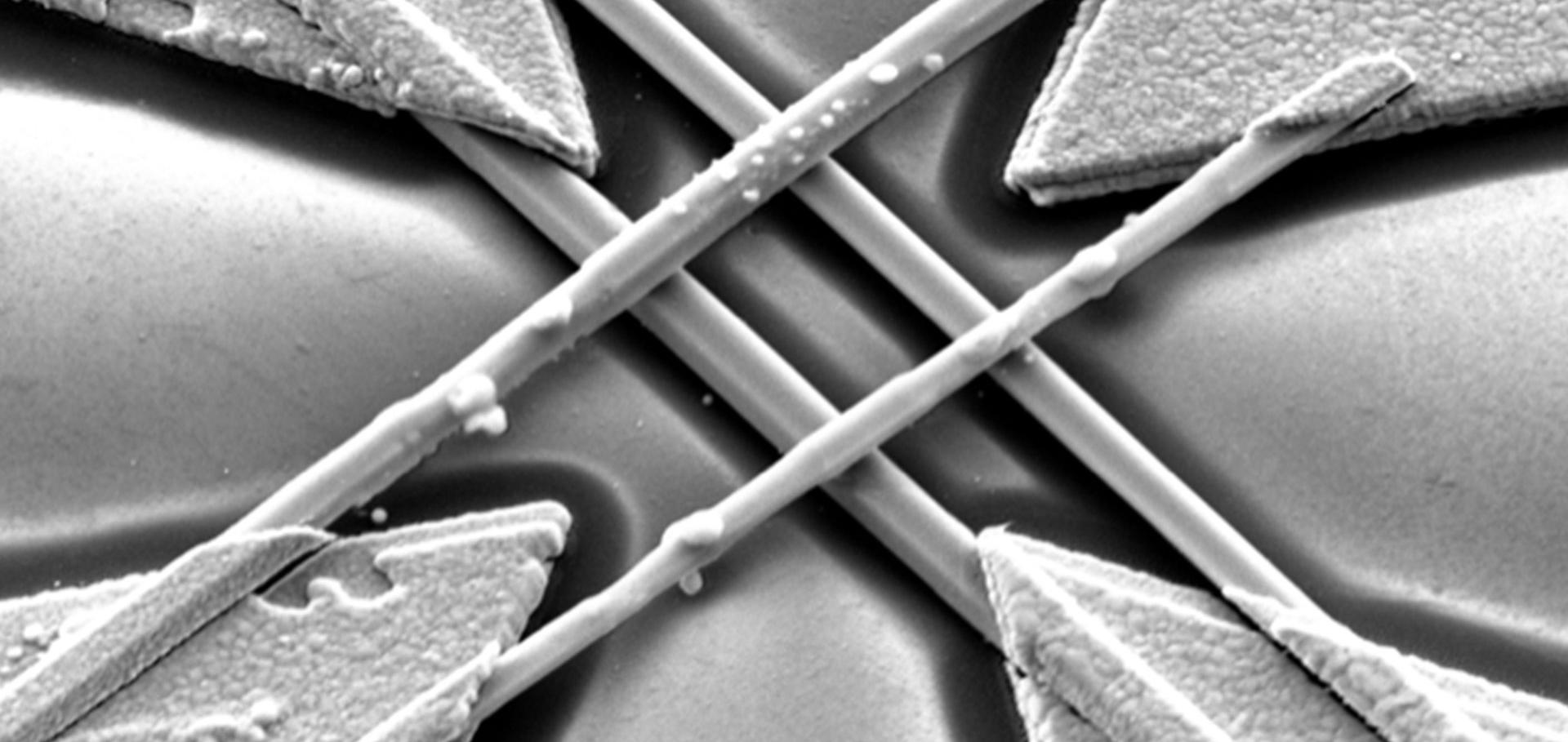
Broadband Phase-Sensitive Single InP Nanowire Photoconductive Terahertz Detectors
Nano Letters American Chemical Society 16:8 (2016) 4925-4931
Abstract:
Terahertz time-domain spectroscopy (THz-TDS) has emerged as a powerful tool for materials characterization and imaging. A trend toward size reduction, higher component integration, and performance improvement for advanced THz-TDS systems is of increasing interest. The use of single semiconducting nanowires for terahertz (THz) detection is a nascent field that has great potential to realize future highly integrated THz systems. In order to develop such components, optimized material optoelectronic properties and careful device design are necessary. Here, we present antenna-optimized photoconductive detectors based on single InP nanowires with superior properties of high carrier mobility (∼1260 cm2 V-1 s-1) and low dark current (∼10 pA), which exhibit excellent sensitivity and broadband performance. We demonstrate that these nanowire THz detectors can provide high quality time-domain spectra for materials characterization in a THz-TDS system, a critical step toward future application in advanced THz-TDS system with high spectral and spatial resolution.Efficient perovskite solar cells by metal ion doping
ENERGY & ENVIRONMENTAL SCIENCE 9:9 (2016) 2892-2901
Electron–phonon coupling in hybrid lead halide perovskites
Nature Communications Nature Publishing Group: Nature Communications 7 (2016)