

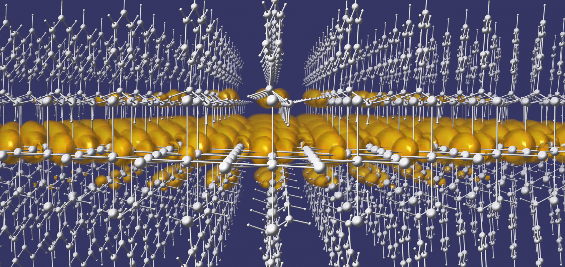

Theory of ab initio downfolding with arbitrary-range electron-phonon coupling
Physical Review B American Physical Society 113:24 (2026) 245144
Abstract:
Ab initio downfolding describes the electronic structure of materials within a low-energy subspace, often around the Fermi level. Typically starting from mean-field calculations, this framework allows for the calculation of one- and two-electron interactions, and the parametrization of a many-body Hamiltonian representing the active space of interest. The subsequent solution of such Hamiltonians can provide insights into the physics of strongly correlated materials. While phonons can substantially screen electron-electron interactions, electron-phonon coupling has been commonly ignored within ab initio downfolding, and when considered, this is done only for short-range coupling. Here we propose a theory of ab initio downfolding that accounts for short- and long-range electron-phonon coupling on equal footing. Our practical computational implementation is readily compatible with current downfolding approaches. We apply our approach to polar materials MgO and GeTe, and we reveal the importance of both short-range and long-range electron-phonon coupling in determining the magnitude of electron-electron interactions. Our results show that in the static limit, phonons reduce the on-site repulsion between electrons by 40% for MgO and by 79% for GeTe. Our framework also predicts that overall attractive nearest-neighbor interactions arise between electrons in GeTe, consistent with superconductivity in this material.Ultrafast spontaneous exciton dissociation via phonon emission in BiVO4
Physical Review Research American Physical Society (APS) 8:1 (2026) 013105
Abstract:
Monoclinic bismuth vanadate ( ) is a promising indirect band gap semiconductor for photoelectrochemical water splitting, yet the characteristics of its low-lying photoexcitations, or excitons, remain poorly understood. Here, we use an Bethe-Salpeter equation approach that incorporates phonon screening to compute the nature and lifetimes of the low-lying excitons of . Our calculations indicate that at 0 K, the lowest-lying exciton energy exceeds the indirect band gap, enabling spontaneous dissociation into free carriers via phonon emission within picoseconds. At 300 K, both phonon emission and absorption effects reduce this timescale to only a few femtoseconds. Phonon screening also greatly reduces the binding energy of the lowest-lying exciton, leading to an optical absorption spectrum that better reproduces experimental measurements. Overall, our findings establish the general conditions under which phonon emission-driven exciton dissociation can occur in indirect gap semiconductors, and they emphasize the critical role phonon screening can play in predictive calculations of photophysical properties of complex materials.Discovery of two new Cu–Sn chalco–halides for potential solar absorber applications
Journal of Materials Chemistry A Royal Society of Chemistry (RSC) (2026)
Abstract:
New compounds are discovered in the under-explored d 10 –s 2 (Cu–Sn) family using exploratory synthesis guided by computational tools. Band-gaps in the visible region with moderate charge-carrier mobilities make these potential solar absorbers. We explore multiple-cation chalco–halide phase fields evaluated by their synthetic accessibility using machine learning models. Exploratory synthesis guided by computational tools leads to the discovery of two new compounds; CuSn 2 SI 3 and Cu 0.35 Sn 5.29 S 2 I 7 , their structures, and electronic and optical properties are reported herein. This is the first report of a stable quaternary compound in the Cu–Sn–S–I phase field. The two new compounds show related crystal structures where Sn 4 S 2 I 4 layers are a common structural motif in both. These Sn 4 S 2 I 4 layers are connected by Cu 2 I 2 layers and disordered Cu–Sn–I layers, forming the three-dimensional structures of CuSn 2 SI 3 and Cu 0.35 Sn 5.29 S 2 I 7 respectively. Electronic band structure calculations using density functional theory show the presence of a direct band gap in CuSn 2 SI 3 and suggest anisotropic transport, in line with the layered structure of the compound. A mixture of the two compounds with ∼86% CuSn 2 SI 3 , shows a band gap in the visible region, close to 2.1 eV and a significant photo-induced charge carrier mobility of ∼1.3 cm 2 V −1 s −1 . This demonstrates Cu–Sn chalco–halides can form a promising phase space to explore for solar absorber materials, with further design and tuning of band gap.Twisted Tin‐Chloride Perovskite Single‐Crystal Heterostructures
Angewandte Chemie International Edition Wiley (2025) e20140
Abstract:
Self‐assembly affords simpler synthetic routes to heterostructures compared with manual layer‐by‐layer stacking, yet controlling interlayer twist angles in a bulk solid remains an outstanding challenge. We report two new single‐crystal heterostructures: (Sn2Cl2)(CYS)2SnCl4 (CYS = +NH3(CH2)2S–; Sn_CYS) and (Sn2Cl2)(SeCYS)2SnCl4 (SeCYS = +NH3(CH2)2Se–; Sn_SeCYS) synthesized in solution, with alternating perovskite and intergrowth layers. Notably, compared to the recently reported lead analog, (Pb2Cl2)(CYS)2PbCl4 (Pb_CYS), the tin heterostructures feature a twist between the perovskite and intergrowth layers. We trace this twist to local distortions at the Sn centers, which change the interfacial lattice‐matching requirements compared to those of the Pb analog. Electronic band structure calculations show that the striking differences in the relative energies of perovskite‐ and intergrowth‐derived bands in Sn_CYS and Pb_CYS arise from structural and not compositional differences. The structural anisotropy of Sn_CYS is also reflected in a large in‐plane photoluminescence linear anisotropy ratio. Interfacial strain further affords differential incorporation of Pb into the perovskite and intergrowth layers of the Sn heterostructures, resulting in redshifted optical absorption onsets. Thus, we posit that local structural distortions may be exploited to manipulate the twist angle and interfacial strain in bulk heterostructures, providing a new handle for tuning the band alignments of bulk quantum‐well electronic structures.Twisted Tin‐Chloride Perovskite Single‐Crystal Heterostructures
Angewandte Chemie (2025)