
Zwitterions in 3D perovskites: organosulfide-halide perovskites
Abstract:
Although sulfide perovskites usually require high-temperature syntheses, we demonstrate that organosulfides can be used in the milder syntheses of halide perovskites. The zwitterionic organosulfide, cysteamine (CYS; +NH3(CH2)2S–), serves as both the X– site and A+ site in the ABX3 halide perovskites, yielding the first examples of 3D organosulfide-halide perovskites: (CYS)PbX2 (X– = Cl– or Br–). Notably, the band structures of (CYS)PbX2 capture the direct bandgaps and dispersive bands of APbX3 perovskites. The sulfur orbitals compose the top of the valence band in (CYS)PbX2, affording unusually small direct bandgaps of 2.31 and 2.16 eV for X– = Cl– and Br–, respectively, falling in the ideal range for the top absorber in a perovskite-based tandem solar cell. Measurements of the carrier dynamics in (CYS)PbCl2 suggest carrier trapping due to defects or lattice distortions. The highly desirable bandgaps, band dispersion, and improved stability of the organosulfide perovskites demonstrated here motivate the continued expansion and exploration of this new family of materials, particularly with respect to extracting photocurrent. Our strategy of combining the A+ and X– sites with zwitterions may offer more members in this family of mixed-anion 3D hybrid perovskites.
Band gaps of halide perovskites from a Wannier-localized optimally tuned screened range-separated hybrid functional
Abstract:
The accurate prediction of the band gaps of halide perovskites within density functional theory is known to be challenging. The recently developed Wannier-localized optimally tuned screened range-separated hybrid functional was shown to be highly accurate for fundamental band gaps of standard semiconductors and insulators. This was achieved by selecting the parameters of the functional to satisfy an ansatz that generalizes the ionization potential theorem to the removal of charge from a state that corresponds to a Wannier function. Here, we present applications of the method to the band gaps of typical halide perovskites. We find a satisfyingly small formal mean absolute error of ∼0.1 eV with respect to experimental band gaps and very good agreement with previous many-body perturbation theory calculations.Understanding the Impact of Dimensional Reduction on the Optoelectronic Properties of Ag/Bi-based Double Perovskites from First Principles
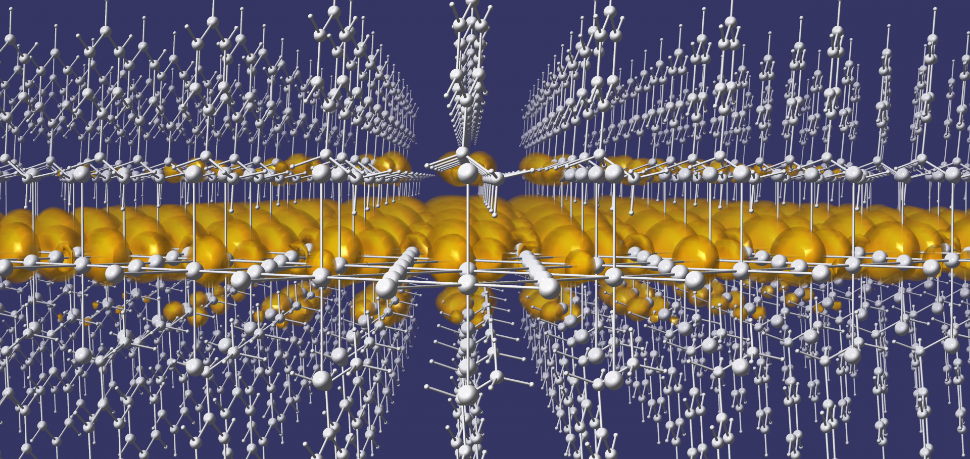
Screening of excitons by organic cations in quasi-two-dimensional organic–inorganic lead-halide perovskites
Abstract:
Interlayer organic cations in quasi-two-dimensional halide perovskites are a versatile tuning vehicle for the optoelectronic properties of these complex systems, but chemical intuition for this design route is yet to be established. Here, we use density functional theory, the GW approximation, and the Bethe-Salpeter equation approach to understand the contribution of the organic cation to the quasiparticle band gap and exciton binding energy of layered perovskites. We show that organic cations in quasi-two-dimensional perovskites contribute significantly to the dielectric screening in these systems, countering quantum confinement effects on the quasiparticle band gap and the exciton binding energy. Using a simple electrostatics model inspired by parallel-plate capacitors, we decouple the organic cation and inorganic layer contributions to the effective dielectric constants and show that dielectric properties of layered perovskites are broadly tunable via the interlayer cation, providing a direct means of tuning photophysical properties for a variety of applications.Optimally tuned starting point for single-shot GW calculations of solids
Abstract:
The dependence of ab initio many-body perturbation theory within the GW approximation on the eigensystem used in calculating quasiparticle corrections limits this method's predictive power. Here, we investigate the accuracy of the recently developed Wannier-localized optimally tuned screened range-separated hybrid (WOT-SRSH) functional as a generalized Kohn-Sham starting point for single-shot GW (G0W0) calculations for a range of semiconductors and insulators. Comparison to calculations based on well-established functionals, namely, PBE, PBE0, and HSE, as well as to self-consistent GW schemes and to experiment, shows that band gaps computed via G0W0@WOT-SRSH have a level of precision and accuracy that is comparable to that of more advanced methods such as quasiparticle self-consistent GW and eigenvalue self-consistent GW. We also find that G0W0@WOT-SRSH improves the description of states deeper in the valence band manifold. Finally, we show that G0W0@WOT-SRSH significantly reduces the sensitivity of computed band gaps to ambiguities in the underlying WOT-SRSH tuning procedure.