Trace Water in Lead Iodide Affecting Perovskite Crystal Nucleation Limits the Performance of Perovskite Solar Cells
Advanced Materials Wiley 36:7 (2024) e2310237
In-situ nanoscopy of carrier dynamics and nanomorphology in metal halide perovskites
Institute of Electrical and Electronics Engineers (IEEE) 00 (2024) 1-2
Factors Enabling Delocalized Charge-Carriers in Pnictogen-Based Solar Absorbers: In-depth Investigation into CuSbSe2
(2024)
Ultrafast Nanoscopy of Single-Grain Morphology and Charge Carrier Dynamics in Metal Halide Perovskites
2024 Conference on Lasers and Electro-Optics, CLEO 2024 (2024)
Abstract:
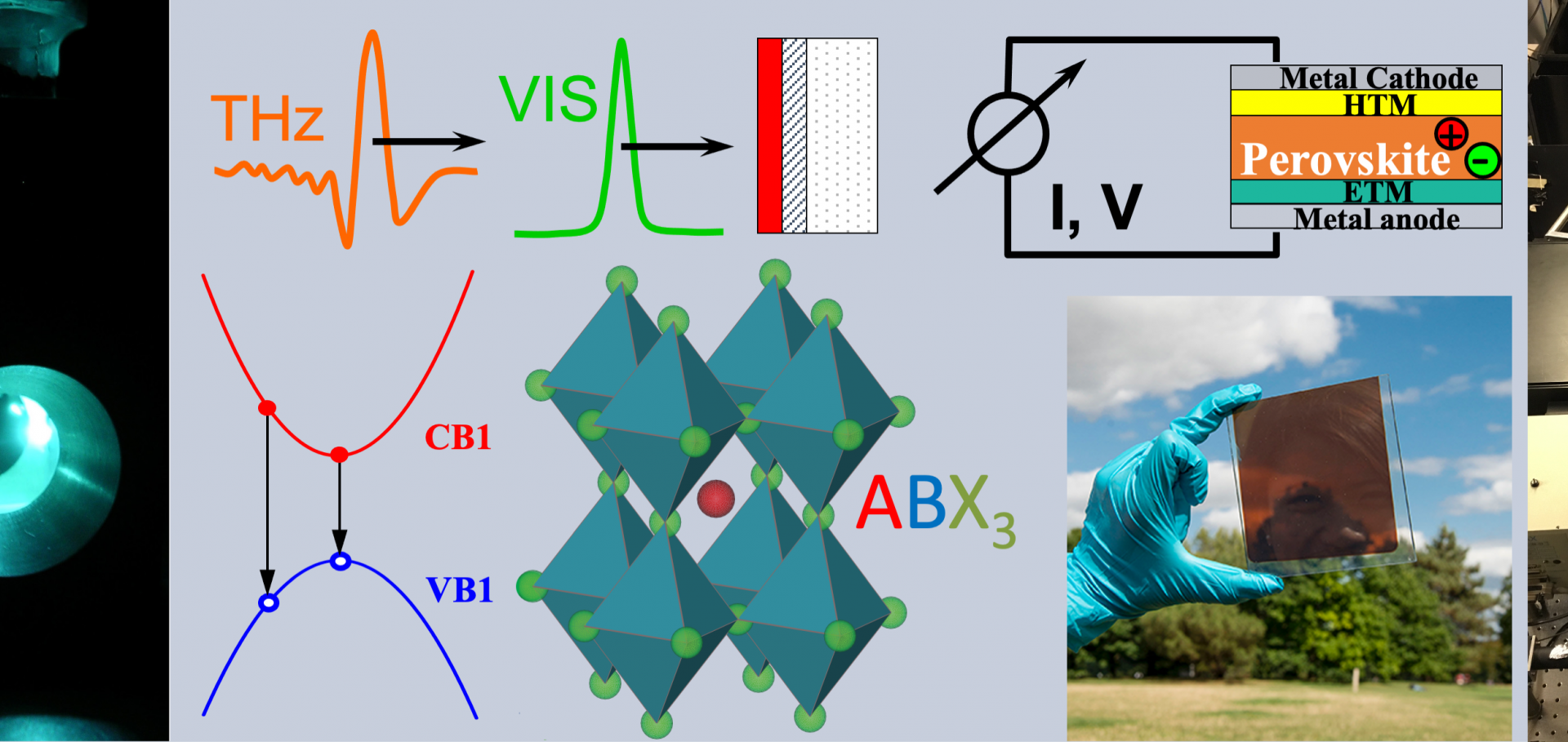
Deep-subcycle shifts of terahertz near-field waveforms reveal the interplay of ultrafast carrier dynamics and nano-morphology in metal halide perovskites. A surprising robustness of out-of-plane diffusion against structural and chemical variations is found on the nanoscale.Ultrafast Nanoscopy of Single-Grain Morphology and Charge Carrier Dynamics in Metal Halide Perovskites
2024 Conference on Lasers and Electro-Optics, CLEO 2024 (2024)