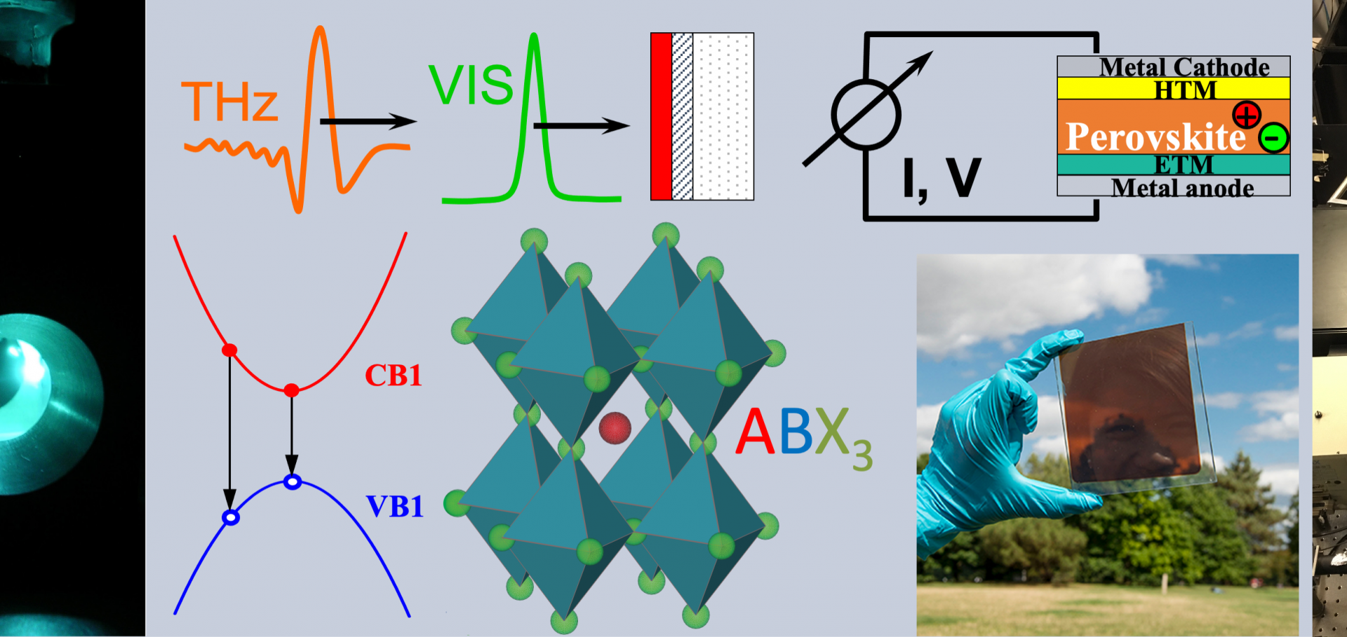
Towards Understanding Long-Range Charge Carrier Transport in 2D Perovkites
Fundacio Scito (2023)
Atomistic understanding of the coherent interface between lead iodide perovskite and lead iodide
Advanced Materials Interfaces Wiley 10:28 (2023) 2300249
Abstract:
Metal halide perovskite semiconductors have shown great performance in solar cells, and including an excess of lead iodide (PbI2) in the thin films, either as mesoscopic particles or embedded domains, often leads to improved solar cell performance. Atomic resolution scanning transmission electron microscope micrographs of formamidinium lead iodide (FAPbI3) perovskite films reveal the FAPbI3:PbI2 interface to be remarkably coherent. It is demonstrated that such interface coherence is achieved by the PbI2 deviating from its common 2H hexagonal phase to form a trigonal 3R polytype through minor shifts in the stacking of the weakly van-der-Waals-bonded layers containing the near-octahedral units. The exact crystallographic interfacial relationship and lattice misfit are revealed. It is further shown that this 3R polytype of PbI2 has similar X-ray diffraction (XRD) peaks to that of the perovskite, making XRD-based quantification of the presence of PbI2 unreliable. Density functional theory demonstrates that this interface does not introduce additional electronic states in the bandgap, making it electronically benign. These findings explain why a slight PbI2 excess during perovskite film growth can help template perovskite crystal growth and passivate interfacial defects, improving solar cell performance.Robust perovskite formation via vacuum thermal annealing for indoor perovskite solar cells
Scientific Reports Nature Research 13:1 (2023) 10933-10933
Abstract:
Perovskite solar cells have rapidly advanced due to their exceptional optoelectronic properties, but achieving uniform crystallization and stability remains challenging. This review examines solvent-assisted annealing, including solvent-vapor and anti-solvent treatments as a strategy to modulate perovskite crystallization for enhanced device performance. Solvent vapors (e.g. DMF, DMSO, alcohol mixtures) introduced during thermal annealing sustain a supersaturated environment that extends nucleation and enables Ostwald ripening, yielding markedly larger grain sizes and improved crystallinity. Studies show that solvent annealing can increase MAPbI3 carrier diffusion lengths beyond 1 μm and maintain >14.5% efficiency even for films up to 1 μm thick. Advanced schemes, such as combined DMSO-water vapor annealing, have produced nearly single-crystal grains and devices with 19.5% power conversion efficiency (PCE), by reducing defect-mediated recombination. These microstructural gains translate into higher PCE and stability: solvent-annealed films exhibit fewer trap sites and inhibited moisture degradation. Finally, we address scalability: ambient solvent-antisolvent treatments have yielded >5 μm grains with 100% film coverage in large-area Perovskite solar cells. Overall, solvent annealing emerges as a powerful tool for tailoring perovskite films. This review synthesizes the mechanisms and performance benefits of solvent annealing and evaluates its prospects for scalable, industrialized PSC fabrication. By identifying key challenges and emerging solutions, it aims to guide future research efforts toward more efficient and manufacturable perovskite solar technologiesChloride-based additive engineering for efficient and stable wide-bandgap perovskite solar cells
Advanced Materials Wiley 35:30 (2023) e2211742
Abstract:
Metal halide perovskite based tandem solar cells are promising to achieve power conversion efficiency beyond the theoretical limit of their single-junction counterparts. However, overcoming the significant open-circuit voltage deficit present in wide-bandgap perovskite solar cells remains a major hurdle for realizing efficient and stable perovskite tandem cells. Here, a holistic approach to overcoming challenges in 1.8 eV perovskite solar cells is reported by engineering the perovskite crystallization pathway by means of chloride additives. In conjunction with employing a self-assembled monolayer as the hole-transport layer, an open-circuit voltage of 1.25 V and a power conversion efficiency of 17.0% are achieved. The key role of methylammonium chloride addition is elucidated in facilitating the growth of a chloride-rich intermediate phase that directs crystallization of the desired cubic perovskite phase and induces more effective halide homogenization. The as-formed 1.8 eV perovskite demonstrates suppressed halide segregation and improved optoelectronic properties.How to Characterize Emerging Luminescent Semiconductors with Unknown Photophysical Properties
PRX Energy American Physical Society (APS) 2:2 (2023)