Dual-source co-evaporation of low-bandgap FA1-xCsxSn1-yPbyI3 perovskites for photovoltaics
Tunable Color Temperatures and Efficient White Emission from Cs2 Ag1- x Nax In1- y Biy Cl6 Double Perovskite Nanocrystals.
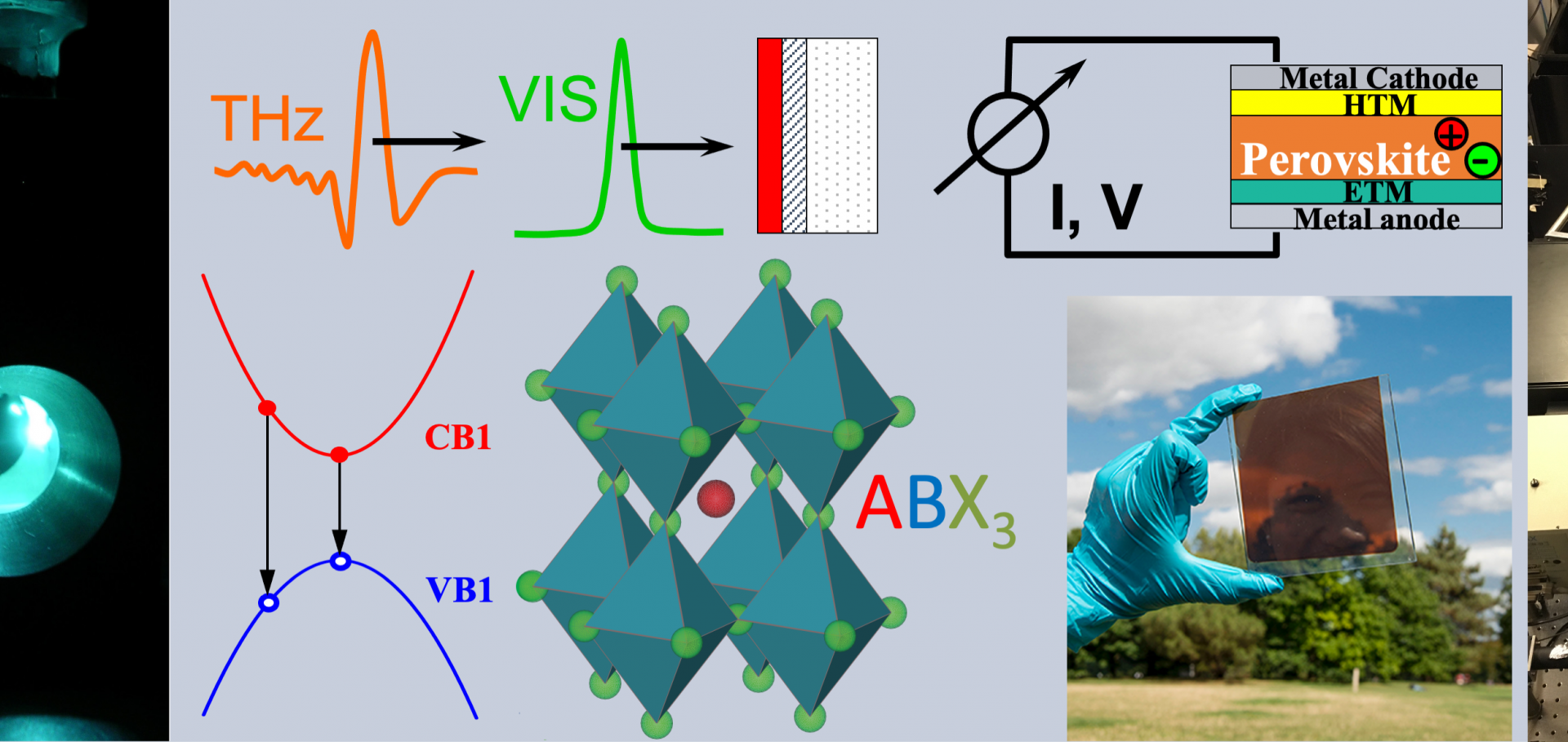
Abstract:
Recently, Bi-doped Cs2 Ag0.6 Na0.4 InCl6 lead-free double perovskites demonstrating efficient warm-white emission have been reported. To enable the solution processing and enrich the application fields of this promising material, here a colloidal synthesis of Cs2 Ag1- x Nax In1- y Biy Cl6 nanocrystals is further developed. Different from its bulk states, the emission color temperatures of the nanocrystal can be tuned from 9759.7 to 4429.2 K by Na+ and Bi3+ incorporation. Furthermore, the newly developed nanocrystals can break the wavefunction symmetry of the self-trapped excitons by partial replacement of Ag+ ions with Na+ ions and consequently allow radiative recombination. Assisted with Bi3+ ions doping and ligand passivation, the photoluminescence quantum yield of the Cs2 Ag0.17 Na0.83 In0.88 Bi0.12 Cl6 nanocrystals is further promoted to 64%, which is the highest value for lead-free perovskite nanocrystals at present. The new colloidal nanocrystals with tunable color temperature and efficient photoluminescence are expected to greatly advance the research progress of lead-free perovskites in single-emitter-based white emitting materials and devices.Charge-carrier cooling and polarization memory loss in formamidinium tin triiodide
Abstract:
Combination of a cryogenic ion-trap machine, operated at 4.7 K, with the free-electron-laser FELIX allows the first experimental characterization of the unusually bright antisymmetric stretch (ν3) and π-bending (ν2) fundamentals of the He–X+–He (X = H, D) chromophore of the in situ prepared HHen+ and DHen+ (n = 3–6) complexes. The band origins obtained are fully supported by first-principles quantum-chemical computations, performed at the MP2, the CCSD(T), and occasionally the CCSDTQ levels employing extended basis sets. Both the experiments and the computations are consistent with structures for the species with n = 3 and 6 being of T-shaped C2v and of D4h symmetry, respectively, while the species with n = 4 are suggested to exhibit interesting dynamical phenomena related to large-amplitude motions.