Home
Department Of Physics text logo
  • Research
    • Our research
    • Our research groups
    • Our research in action
    • Research funding support
    • Summer internships for undergraduates
  • Study
    • Undergraduates
    • Postgraduates
  • Engage
    • For alumni
    • For business
    • For schools
    • For the public
Menu
CMP
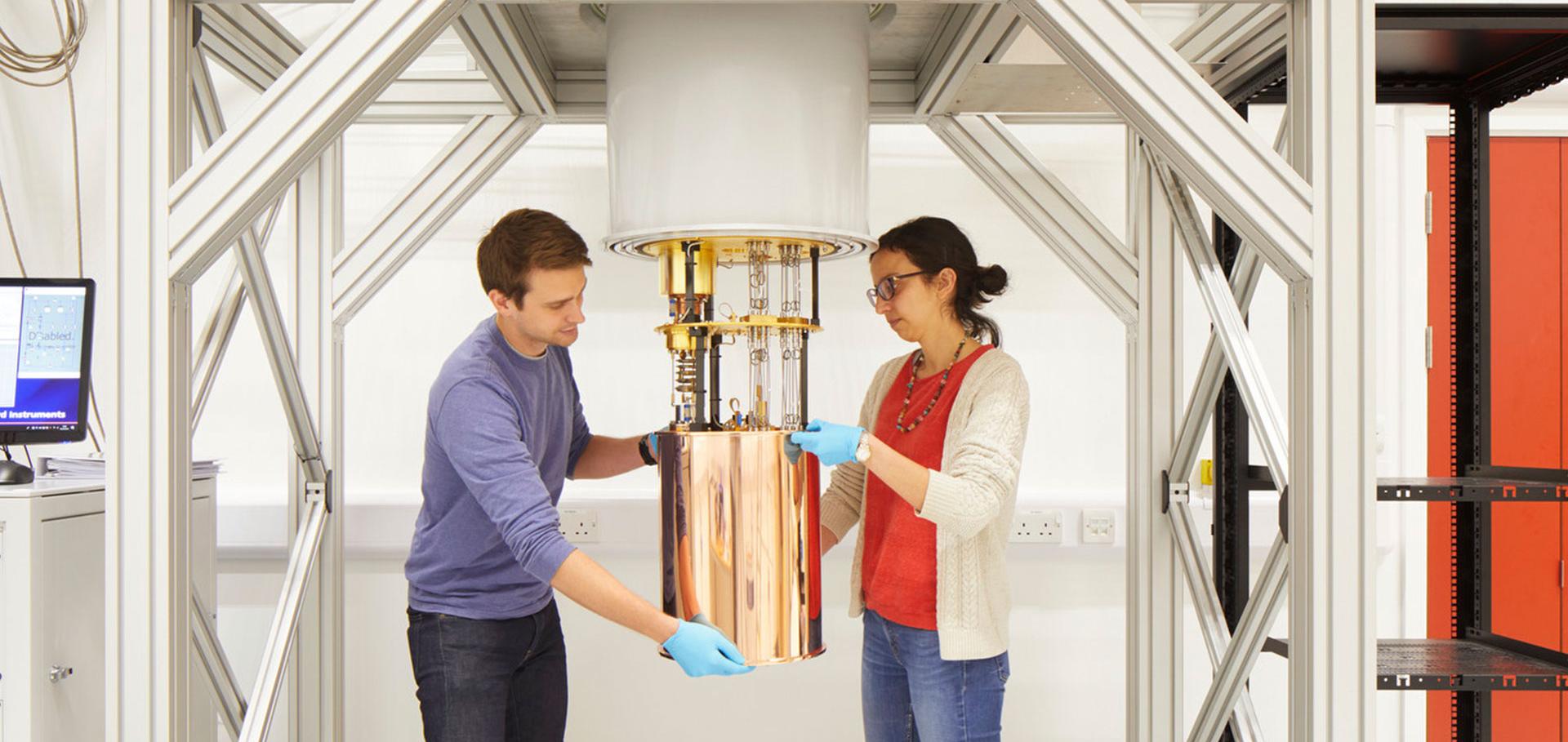
Credit: Jack Hobhouse

Prof Yen-Hung Lin

Long Term Visitor

Sub department

  • Condensed Matter Physics
yen-hung.lin@physics.ox.ac.uk
Telephone: 01865 (2)82328
Robert Hooke Building, room G26
  • About
  • Publications

Solution-processed p-type copper(I) thiocyanate (CuSCN) for low-voltage flexible thin-film transistors and integrated inverter circuits

Applied Physics Letters AIP Publishing 110:11 (2017) 113504

Authors:

Luisa Petti, Pichaya Pattanasattayavong, Yen-Hung Lin, Niko Münzenrieder, Giuseppe Cantarella, Nir Yaacobi-Gross, Feng Yan, Gerhard Tröster, Thomas D Anthopoulos
More details from the publisher

Heterojunction oxide thin-film transistors with unprecedented electron mobility grown from solution.

Science advances 3:3 (2017) e1602640

Authors:

Hendrik Faber, Satyajit Das, Yen-Hung Lin, Nikos Pliatsikas, Kui Zhao, Kui Zhao, Thomas Kehagias, George Dimitrakopulos, Aram Amassian, Panos A Patsalas, Thomas D Anthopoulos

Abstract:

Thin-film transistors made of solution-processed metal oxide semiconductors hold great promise for application in the emerging sector of large-area electronics. However, further advancement of the technology is hindered by limitations associated with the extrinsic electron transport properties of the often defect-prone oxides. We overcome this limitation by replacing the single-layer semiconductor channel with a low-dimensional, solution-grown In2O3/ZnO heterojunction. We find that In2O3/ZnO transistors exhibit band-like electron transport, with mobility values significantly higher than single-layer In2O3 and ZnO devices by a factor of 2 to 100. This marked improvement is shown to originate from the presence of free electrons confined on the plane of the atomically sharp heterointerface induced by the large conduction band offset between In2O3 and ZnO. Our finding underscores engineering of solution-grown metal oxide heterointerfaces as an alternative strategy to thin-film transistor development and has the potential for widespread technological applications.
More details from the publisher
More details
More details

Sub-second photonic processing of solution-deposited single layer and heterojunction metal oxide thin-film transistors using a high-power xenon flash lamp

Journal of Materials Chemistry C Royal Society of Chemistry (RSC) 5:45 (2017) 11724-11732

Authors:

Kornelius Tetzner, Yen-Hung Lin, Anna Regoutz, Akmaral Seitkhan, David J Payne, Thomas D Anthopoulos
More details from the publisher
More details

Doping of Large Ionization Potential Indenopyrazine Polymers via Lewis Acid Complexation with Tris(pentafluorophenyl)borane: A Simple Method for Improving the Performance of Organic Thin-Film Transistors

Chemistry of Materials American Chemical Society (ACS) 28:21 (2016) 8016-8024

Authors:

Yang Han, George Barnes, Yen-Hung Lin, Jaime Martin, Mohammed Al-Hashimi, Siham Y AlQaradawi, Thomas D Anthopoulos, Martin Heeney
More details from the publisher

Nondestructive Method for Mapping Metal Contact Diffusion in In2O3 Thin-Film Transistors.

ACS applied materials & interfaces 8:38 (2016) 25631-25636

Authors:

Olga Kryvchenkova, Isam Abdullah, John Emyr Macdonald, Martin Elliott, Thomas D Anthopoulos, Yen-Hung Lin, Petar Igić, Karol Kalna, Richard J Cobley

Abstract:

The channel width-to-length ratio is an important transistor parameter for integrated circuit design. Contact diffusion into the channel during fabrication or operation alters the channel width and this important parameter. A novel methodology combining atomic force microscopy and scanning Kelvin probe microscopy (SKPM) with self-consistent modeling is developed for the nondestructive detection of contact diffusion on active devices. Scans of the surface potential are modeled using physically based Technology Computer Aided Design (TCAD) simulations when the transistor terminals are grounded and under biased conditions. The simulations also incorporate the tip geometry to investigate its effect on the measurements due to electrostatic tip-sample interactions. The method is particularly useful for semiconductor- and metal-semiconductor interfaces where the potential contrast resulting from dopant diffusion is below that usually detectable with scanning probe microscopy.
More details from the publisher
More details
More details

Pagination

  • First page First
  • Previous page Prev
  • …
  • Page 12
  • Page 13
  • Page 14
  • Page 15
  • Current page 16
  • Page 17
  • Page 18
  • Page 19
  • Page 20
  • Next page Next
  • Last page Last

Footer Menu

  • Contact us
  • Giving to the Dept of Physics
  • Work with us
  • Media

User account menu

  • Log in

Follow us

FIND US

Clarendon Laboratory,

Parks Road,

Oxford,

OX1 3PU

CONTACT US

Tel: +44(0)1865272200

University of Oxfrod logo Department Of Physics text logo
IOP Juno Champion logo Athena Swan Silver Award logo

© University of Oxford - Department of Physics

Cookies | Privacy policy | Accessibility statement

Built by: Versantus

  • Home
  • Research
  • Study
  • Engage
  • Our people
  • News & Comment
  • Events
  • Our facilities & services
  • About us
  • Current students
  • Staff intranet