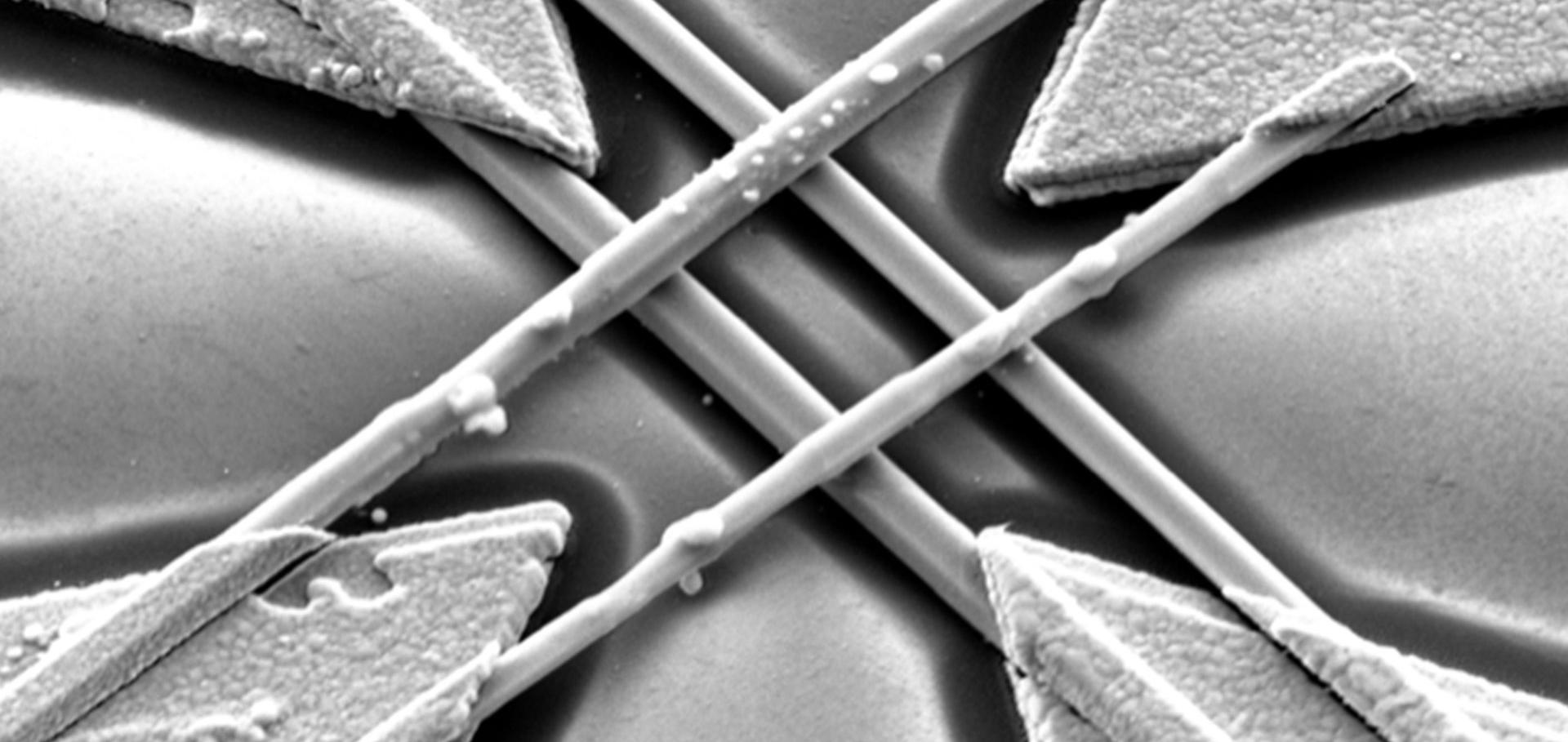
Electronic properties of GaAs, InAs and InP nanowires studied by terahertz spectroscopy.
Nanotechnology 24:21 (2013) 214006
Abstract:
We have performed a comparative study of ultrafast charge carrier dynamics in a range of III-V nanowires using optical pump-terahertz probe spectroscopy. This versatile technique allows measurement of important parameters for device applications, including carrier lifetimes, surface recombination velocities, carrier mobilities and donor doping levels. GaAs, InAs and InP nanowires of varying diameters were measured. For all samples, the electronic response was dominated by a pronounced surface plasmon mode. Of the three nanowire materials, InAs nanowires exhibited the highest electron mobilities of 6000 cm² V⁻¹ s⁻¹, which highlights their potential for high mobility applications, such as field effect transistors. InP nanowires exhibited the longest carrier lifetimes and the lowest surface recombination velocity of 170 cm s⁻¹. This very low surface recombination velocity makes InP nanowires suitable for applications where carrier lifetime is crucial, such as in photovoltaics. In contrast, the carrier lifetimes in GaAs nanowires were extremely short, of the order of picoseconds, due to the high surface recombination velocity, which was measured as 5.4 × 10⁵ cm s⁻¹. These findings will assist in the choice of nanowires for different applications, and identify the challenges in producing nanowires suitable for future electronic and optoelectronic devices.Dependence of dye regeneration and charge collection on the pore-filling fraction in solid-state dye-sensitized solar cells
Advanced Functional Materials (2013)
Abstract:
Solid-state dye-sensitized solar cells rely on effective infiltration of a solid-state hole-transporting material into the pores of a nanoporous TiO network to allow for dye regeneration and hole extraction. Using microsecond transient absorption spectroscopy and femtosecond photoluminescence upconversion spectroscopy, the hole-transfer yield from the dye to the hole-transporting material 2,2',7,7'-tetrakis(N,N-di-p-methoxyphenylamine)-9,9'-spirobifluorene (spiro-OMeTAD) is shown to rise rapidly with higher pore-filling fractions as the dye-coated pore surface is increasingly covered with hole-transporting material. Once a pore-filling fraction of ≈30% is reached, further increases do not significantly change the hole-transfer yield. Using simple models of infiltration of spiro-OMeTAD into the TiO porous network, it is shown that this pore-filling fraction is less than the amount required to cover the dye surface with at least a single layer of hole-transporting material, suggesting that charge diffusion through the dye monolayer network precedes transfer to the hole-transporting material. Comparison of these results with device parameters shows that improvements of the power-conversion efficiency beyond ≈30% pore filling are not caused by a higher hole-transfer yield, but by a higher charge-collection efficiency, which is found to occur in steps. The observed sharp onsets in photocurrent and power-conversion efficiencies with increasing pore-filling fraction correlate well with percolation theory, predicting the points of cohesive pathway formation in successive spiro-OMeTAD layers adhered to the pore walls. From percolation theory it is predicted that, for standard mesoporous TiO with 20 nm pore size, the photocurrent should show no further improvement beyond an ≈83% pore-filling fraction. Solid-state dye-sensitized solar cells capable of complete hole transfer with pore-filling fractions as low as ∼30% are demonstrated. Improvements of device efficiencies beyond ∼30% are explained by a stepwise increase in charge-collection efficiency in agreement with percolation theory. Furthermore, it is predicted that, for a 20 nm pore size, the photocurrent reaches a maximum at ∼83% pore-filling fraction. © 2013 WILEY-VCH Verlag GmbH & Co. KGaA, Weinheim.High Charge Carrier Mobilities and Lifetimes in Organolead Trihalide Perovskites
Advanced Materials (2013)
Novel single-walled carbon nanotube: Dual polymer nanostructures
ABSTRACTS OF PAPERS OF THE AMERICAN CHEMICAL SOCIETY 245 (2013)
Strong carrier lifetime enhancement in GaAs nanowires coated with semiconducting polymer.
Nano Lett 12:12 (2012) 6293-6301