Optimizing the energy offset between dye and hole-transporting material in solid-state dye-sensitized solar cells
Journal of Physical Chemistry C 117:39 (2013) 19850-19858
Abstract:
The power-conversion efficiency of solid-state dye-sensitized solar cells can be optimized by reducing the energy offset between the highest occupied molecular orbital (HOMO) levels of dye and hole-transporting material (HTM) to minimize the loss-in-potential. Here, we report a study of three novel HTMs with HOMO levels slightly above and below the one of the commonly used HTM 2,2′,7,7′- tetrakis(N,N-di-p-methoxyphenylamino)-9,9′- spirobifluorene (spiro-OMeTAD) to systematically explore this possibility. Using transient absorption spectroscopy and employing the ruthenium based dye Z907 as sensitizer, it is shown that, despite one new HTM showing a 100% hole-transfer yield, all devices based on the new HTMs performed worse than those incorporating spiro-OMeTAD. We further demonstrate that the design of the HTM has an additional impact on the electronic density of states present at the TiO2 electrode surface and hence influences not only hole- but also electron-transfer from the sensitizer. These results provide insight into the complex influence of the HTM on charge transfer and provide guidance for the molecular design of new materials. © 2013 American Chemical Society.Efficient planar heterojunction perovskite solar cells by vapour deposition
Nature 501:7467 (2013) 395-398
Abstract:
Many different photovoltaic technologies are being developed for large-scale solar energy conversion. The wafer-based first-generation photovoltaic devices have been followed by thin-film solid semiconductor absorber layers sandwiched between two charge-selective contacts and nanostructured (or mesostructured) solar cells that rely on a distributed heterojunction to generate charge and to transport positive and negative charges in spatially separated phases. Although many materials have been used in nanostructured devices, the goal of attaining high-efficiency thin-film solar cells in such a way has yet to be achieved. Organometal halide perovskites have recently emerged as a promising material for high-efficiency nanostructured devices. Here we show that nanostructuring is not necessary to achieve high efficiencies with this material: a simple planar heterojunction solar cell incorporating vapour-deposited perovskite as the absorbing layer can have solar-to-electrical power conversion efficiencies of over 15 per cent (as measured under simulated full sunlight). This demonstrates that perovskite absorbers can function at the highest efficiencies in simplified device architectures, without the need for complex nanostructures. © 2013 Macmillan Publishers Limited. All rights reserved.Direct observation of charge-carrier heating at WZ-ZB InP nanowire heterojunctions.
Nano Lett 13:9 (2013) 4280-4287
Abstract:
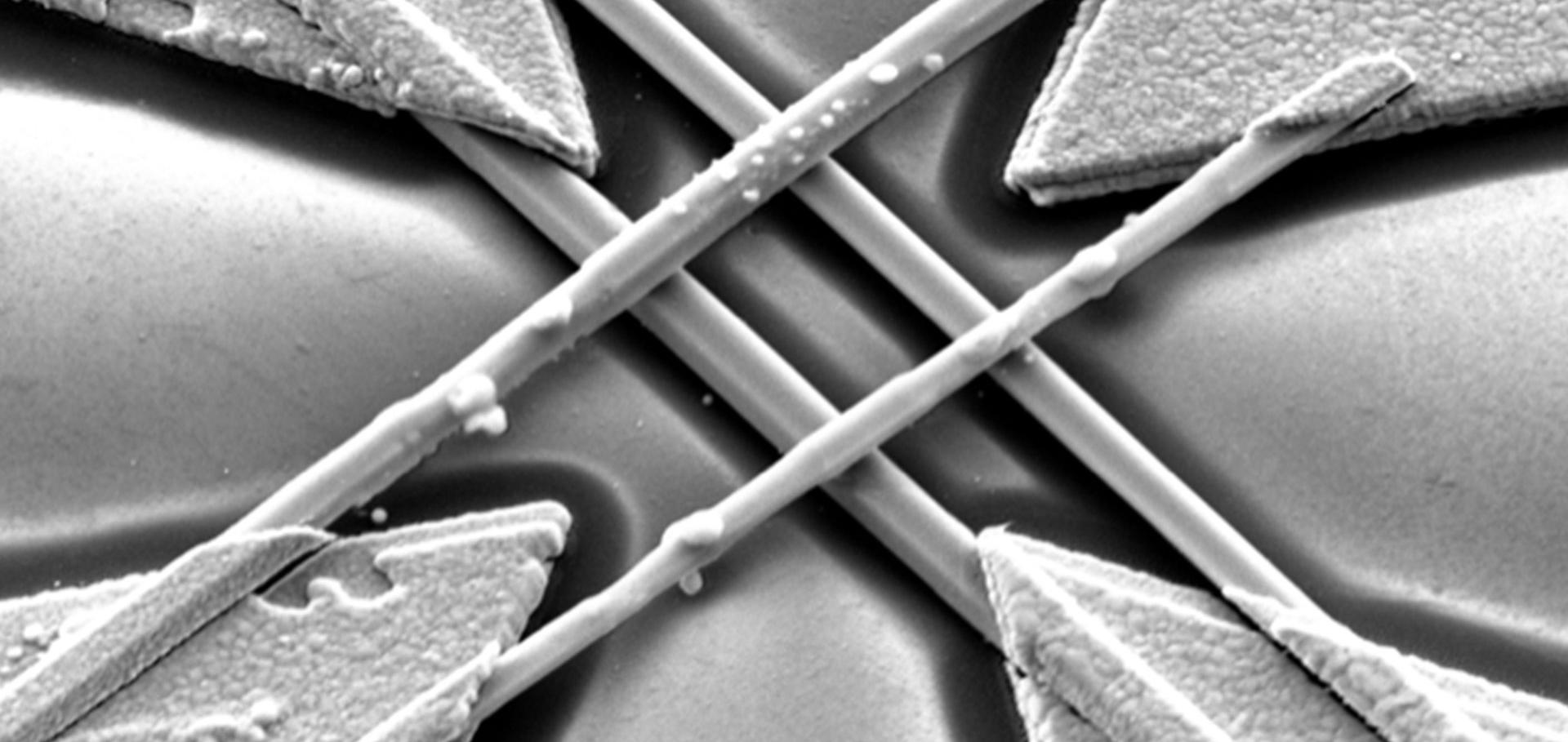
We have investigated the dynamics of hot charge carriers in InP nanowire ensembles containing a range of densities of zinc-blende inclusions along the otherwise wurtzite nanowires. From time-dependent photoluminescence spectra, we extract the temperature of the charge carriers as a function of time after nonresonant excitation. We find that charge-carrier temperature initially decreases rapidly with time in accordance with efficient heat transfer to lattice vibrations. However, cooling rates are subsequently slowed and are significantly lower for nanowires containing a higher density of stacking faults. We conclude that the transfer of charges across the type II interface is followed by release of additional energy to the lattice, which raises the phonon bath temperature above equilibrium and impedes the carrier cooling occurring through interaction with such phonons. These results demonstrate that type II heterointerfaces in semiconductor nanowires can sustain a hot charge-carrier distribution over an extended time period. In photovoltaic applications, such heterointerfaces may hence both reduce recombination rates and limit energy losses by allowing hot-carrier harvesting.Electronic properties of GaAs, InAs and InP nanowires studied by terahertz spectroscopy.
Nanotechnology 24:21 (2013) 214006
Abstract:
We have performed a comparative study of ultrafast charge carrier dynamics in a range of III-V nanowires using optical pump-terahertz probe spectroscopy. This versatile technique allows measurement of important parameters for device applications, including carrier lifetimes, surface recombination velocities, carrier mobilities and donor doping levels. GaAs, InAs and InP nanowires of varying diameters were measured. For all samples, the electronic response was dominated by a pronounced surface plasmon mode. Of the three nanowire materials, InAs nanowires exhibited the highest electron mobilities of 6000 cm² V⁻¹ s⁻¹, which highlights their potential for high mobility applications, such as field effect transistors. InP nanowires exhibited the longest carrier lifetimes and the lowest surface recombination velocity of 170 cm s⁻¹. This very low surface recombination velocity makes InP nanowires suitable for applications where carrier lifetime is crucial, such as in photovoltaics. In contrast, the carrier lifetimes in GaAs nanowires were extremely short, of the order of picoseconds, due to the high surface recombination velocity, which was measured as 5.4 × 10⁵ cm s⁻¹. These findings will assist in the choice of nanowires for different applications, and identify the challenges in producing nanowires suitable for future electronic and optoelectronic devices.Dependence of dye regeneration and charge collection on the pore-filling fraction in solid-state dye-sensitized solar cells
Advanced Functional Materials (2013)