Efficient, semitransparent neutral-colored solar cells based on microstructured formamidinium lead trihalide perovskite.
Journal of Physical Chemistry Letters American Chemical Society 6:1 (2015) 129-138
Abstract:
Efficient, neutral-colored semitransparent solar cells are of commercial interest for incorporation into the windows and surfaces of buildings and automobiles. Here, we report on semitransparent perovskite solar cells that are both efficient and neutral-colored, even in full working devices. Using the microstructured architecture previously developed, we achieve higher efficiencies by replacing methylammonium lead iodide perovskite with formamidinium lead iodide. Current-voltage hysteresis is also much reduced. Furthermore, we apply a novel transparent cathode to the devices, enabling us to fabricate neutral-colored semitransparent full solar cells for the first time. Such devices demonstrate over 5% power conversion efficiency for average visible transparencies of almost 30%, retaining impressive color-neutrality. This makes these devices the best-performing single-junction neutral-colored semitransparent solar cells to date. These microstructured perovskite solar cells are shown to have a significant advantage over silicon solar cells in terms of performance at high incident angles of sunlight, making them ideal for building integration.FTU Diagnostic System Based on THz Time-domain Spectroscopy
Physics Procedia Elsevier 62 (2015) 65-70
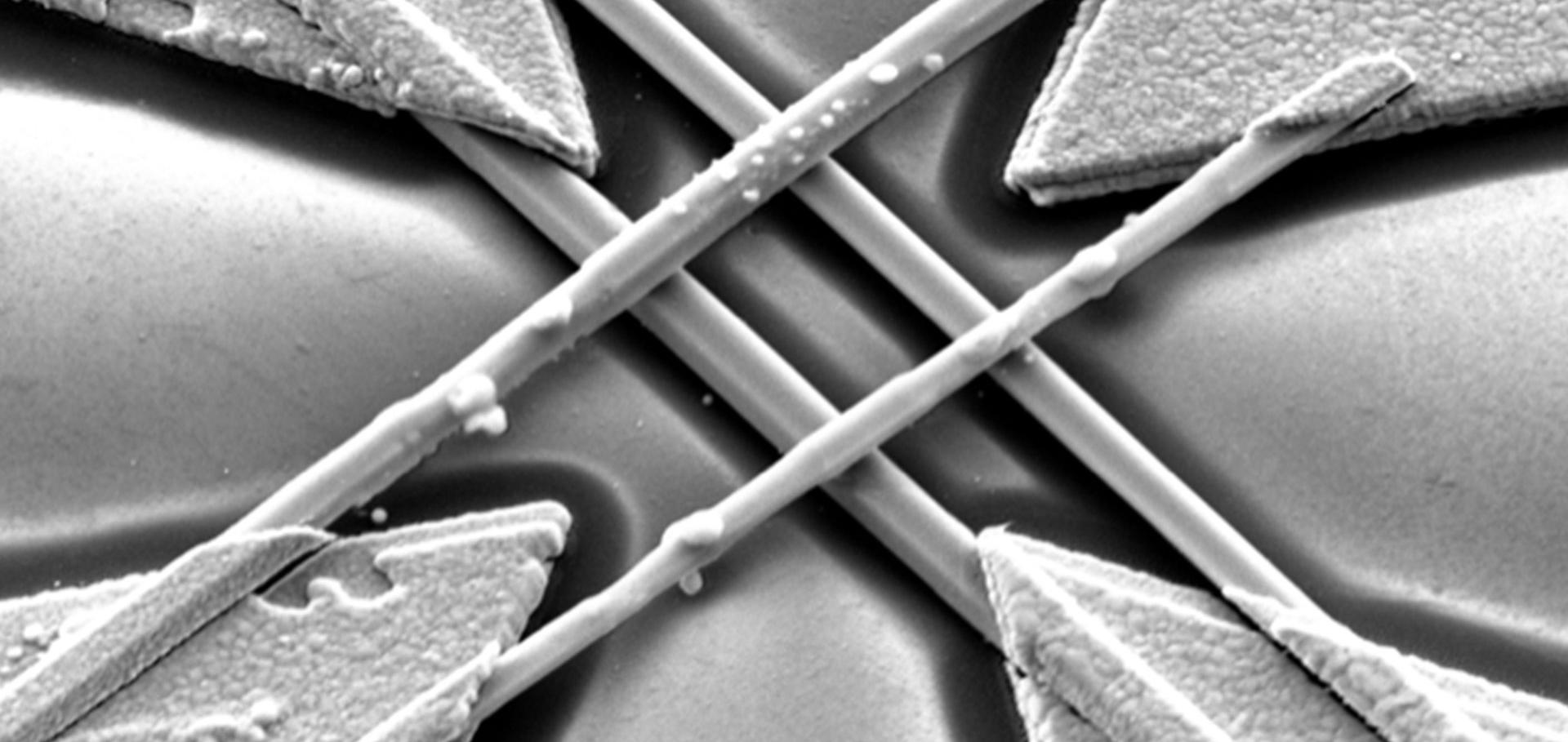
Single Nanowire Terahertz Detectors
Optica Publishing Group (2015) stu4h.8
Optical properties and limiting photocurrent of thin-film perovskite solar cells
Energy and Environmental Science Royal Society of Chemistry 8:2 (2014) 602-609
Abstract:
Metal-halide perovskite light-absorbers have risen to the forefront of photovoltaics research offering the potential to combine low-cost fabrication with high power-conversion efficiency. Much of the development has been driven by empirical optimisation strategies to fully exploit the favourable electronic properties of the absorber layer. To build on this progress, a full understanding of the device operation requires a thorough optical analysis of the device stack, providing a platform for maximising the power conversion efficiency through a precise determination of parasitic losses caused by coherence and absorption in the non-photoactive layers. Here we use an optical model based on the transfer-matrix formalism for analysis of perovskite-based planar heterojunction solar cells using experimentally determined complex refractive index data. We compare the modelled properties to experimentally determined data, and obtain good agreement, revealing that the internal quantum efficiency in the solar cells approaches 100%. The modelled and experimental dependence of the photocurrent on incidence angle exhibits only a weak variation, with very low reflectivity losses at all angles, highlighting the potential for useful power generation over a full daylight cycle.Measurement of doping concentration, internal quantum efficiency and non-radiative lifetime of InP nanowires
Institute of Electrical and Electronics Engineers (IEEE) (2014) 272-274