Single GaAs/AlGaAs Nanowire Photoconductive Terahertz Detectors
Institute of Electrical and Electronics Engineers (IEEE) (2014) 221-222
Ultrafast transient terahertz conductivity of monolayer MoS₂ and WSe₂ grown by chemical vapor deposition
ACS nano American Chemical Society 8:11 (2014) 11147-11153
Abstract:
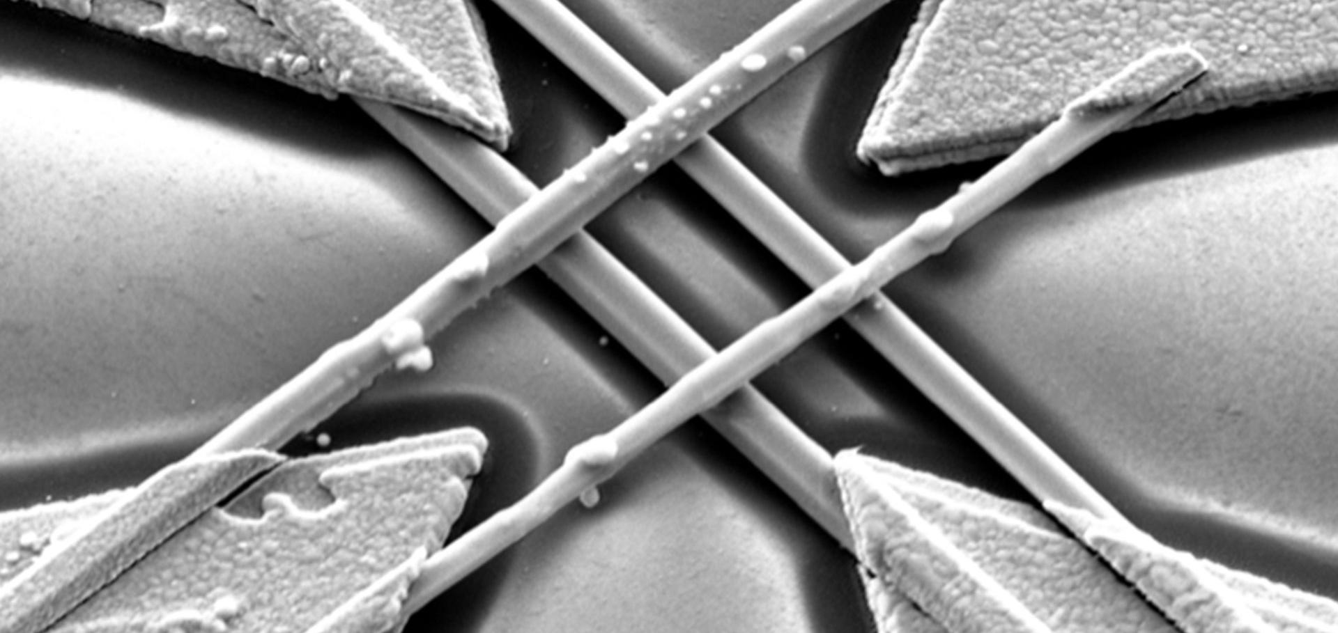
We have measured ultrafast charge carrier dynamics in monolayers and trilayers of the transition metal dichalcogenides MoS2 and WSe2 using a combination of time-resolved photoluminescence and terahertz spectroscopy. We recorded a photoconductivity and photoluminescence response time of just 350 fs from CVD-grown monolayer MoS2, and 1 ps from trilayer MoS2 and monolayer WSe2. Our results indicate the potential of these materials as high-speed optoelectronic materials.Electron mobilities approaching bulk limits in "surface-free" GaAs nanowires.
Nano letters American Chemical Society 14:10 (2014) 5989-5994
Abstract:
Achieving bulk-like charge carrier mobilities in semiconductor nanowires is a major challenge facing the development of nanowire-based electronic devices. Here we demonstrate that engineering the GaAs nanowire surface by overcoating with optimized AlGaAs shells is an effective means of obtaining exceptionally high carrier mobilities and lifetimes. We performed measurements of GaAs/AlGaAs core-shell nanowires using optical pump-terahertz probe spectroscopy: a noncontact and accurate probe of carrier transport on ultrafast time scales. The carrier lifetimes and mobilities both improved significantly with increasing AlGaAs shell thickness. Remarkably, optimized GaAs/AlGaAs core-shell nanowires exhibited electron mobilities up to 3000 cm(2) V(-1) s(-1), reaching over 65% of the electron mobility typical of high quality undoped bulk GaAs at equivalent photoexcited carrier densities. This points to the high interface quality and the very low levels of ionized impurities and lattice defects in these nanowires. The improvements in mobility were concomitant with drastic improvements in photoconductivity lifetime, reaching 1.6 ns. Comparison of photoconductivity and photoluminescence dynamics indicates that midgap GaAs surface states, and consequently surface band-bending and depletion, are effectively eliminated in these high quality heterostructures.Solution deposition-conversion for planar heterojunction mixed halide perovskite solar cells
Advanced Energy Materials 4:14 (2014)
Abstract:
Solution-deposited-converted perovskite solar cells are studied by converting PbISolution Deposition‐Conversion for Planar Heterojunction Mixed Halide Perovskite Solar Cells
Advanced Energy Materials Wiley 4:14 (2014)